Teardown report: DELL 165W PD3.1 gallium nitride power adapter LA165PM210
Preface
Charging Head Network purchased a laptop power adapter launched by Dell . This adapter uses gallium nitride technology and supports PD3.1 fast charging. The output supports Dell 28V 5.85A 165W , 20V 6.5A 130W private protocol, and supports 140W PD3. 1 spec. The adapter uses a plum blossom interface for power supply and comes with a 1.8-meter-long USB-C interface output cable. You can choose power cables of different lengths according to the use environment, which is neat and beautiful.
The adapter adopts the Dell family style and has an indicator light for power indication. This adapter uses active rectification to reduce losses and has a built-in Infineon gallium nitride switch tube. In addition, an Infineon hybrid flyback controller is used to improve conversion efficiency. The following is a disassembly of this gallium nitride power adapter, analyzing the internal solutions and materials.
Dell 165W GaN power adapter appearance

Dell’s 165W gallium nitride power adapter has a separate wire body design. The power cord pins are protected by a plastic shell. The whole body is wound several times and then fixed with a paper ring.
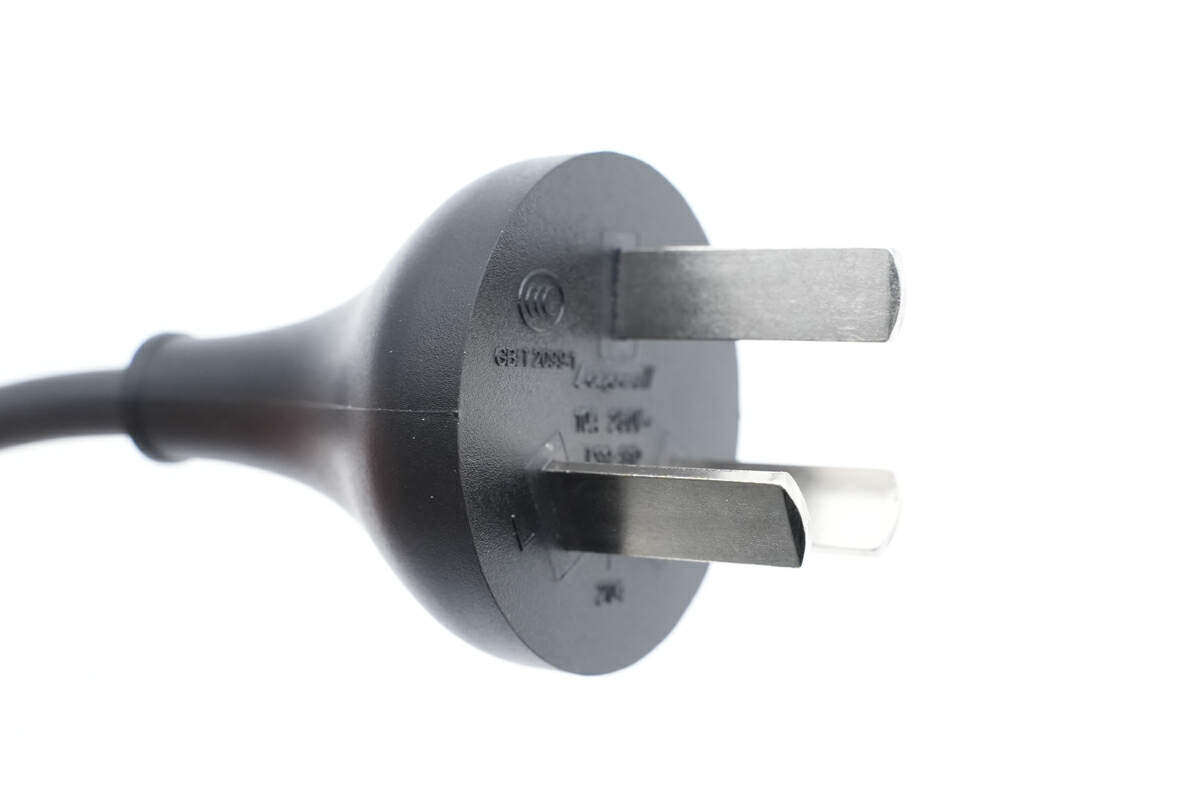
The power cord adopts a three-pin national standard plug, which can be grounded to effectively prevent users from getting electric shock.
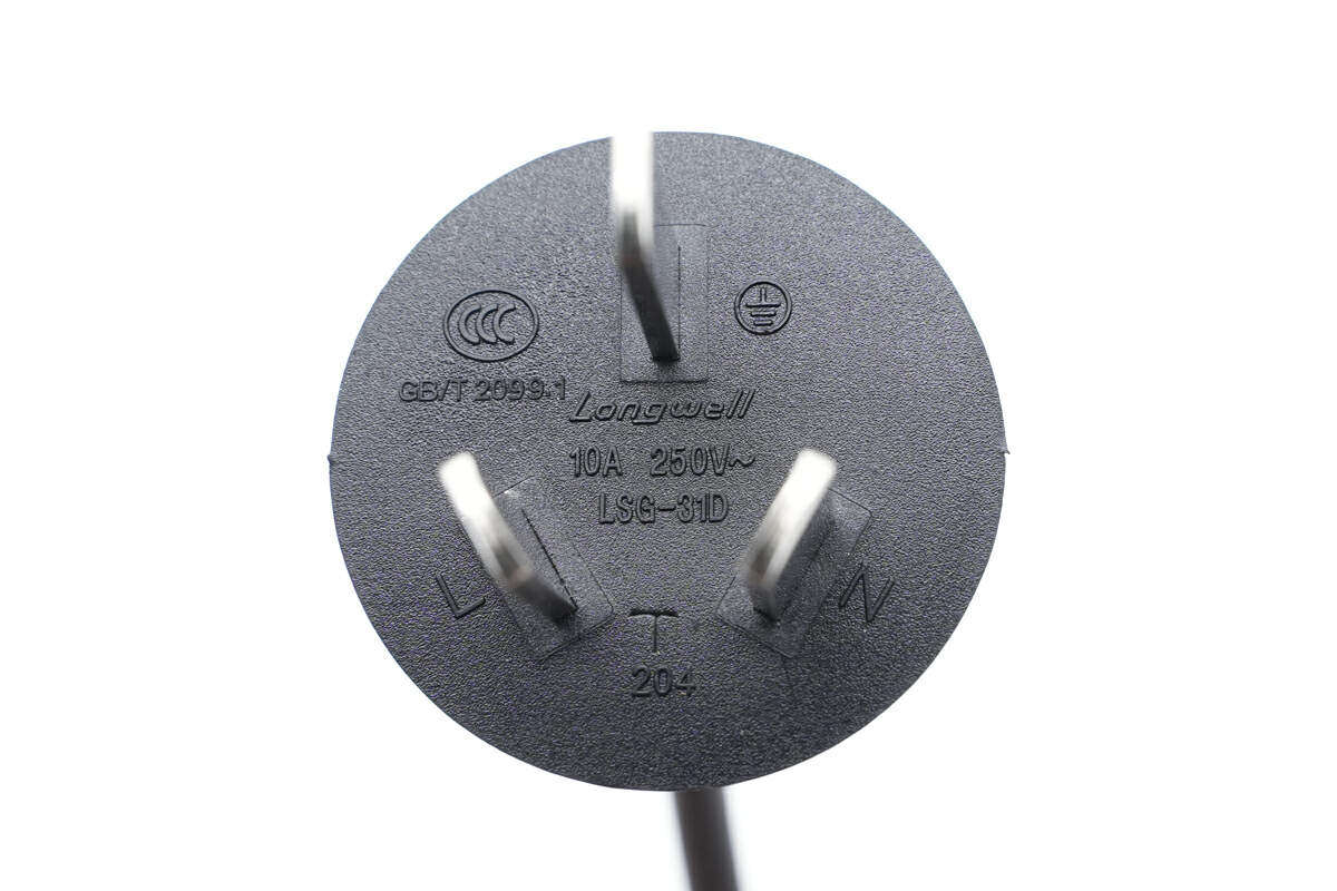
The power cord manufacturer is LONGWELL, the specification is 10A 250V~, and it has passed CCC certification.
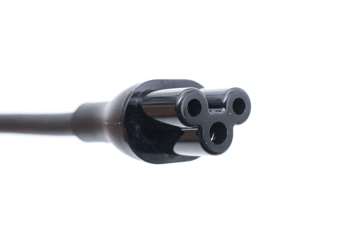
The other end of the power cord is a plum blossom plug, and the outer casing is designed with a bright finish.
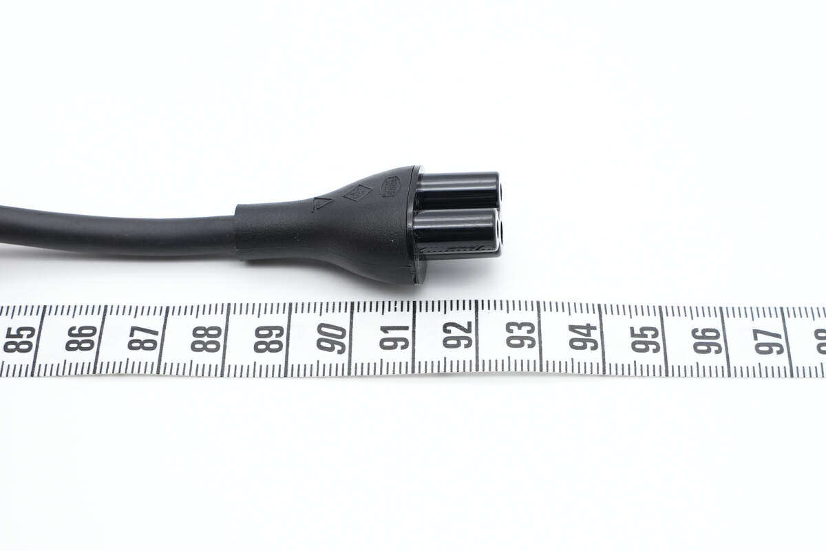
The measured length of the power cord is approximately 92cm.
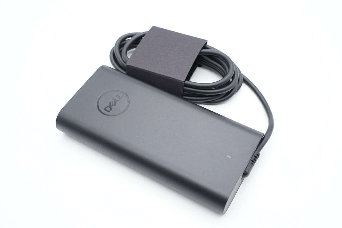
The power adapter adopts a straight shape with semi-circular arc designs on both sides. The output comes with a USB-C cable. The overall design is a very classic Dell power supply style.
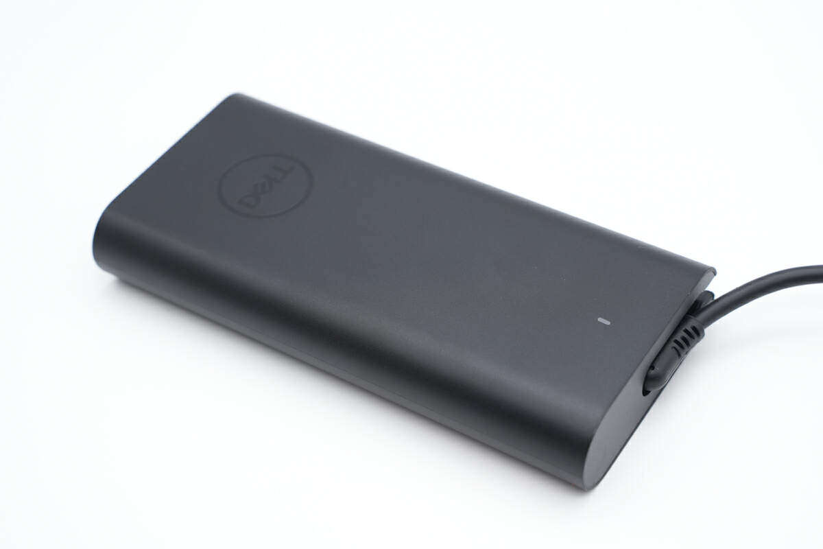
The body is made of PC fireproof plastic shell, and the surface is frosted to effectively resist fingerprints.
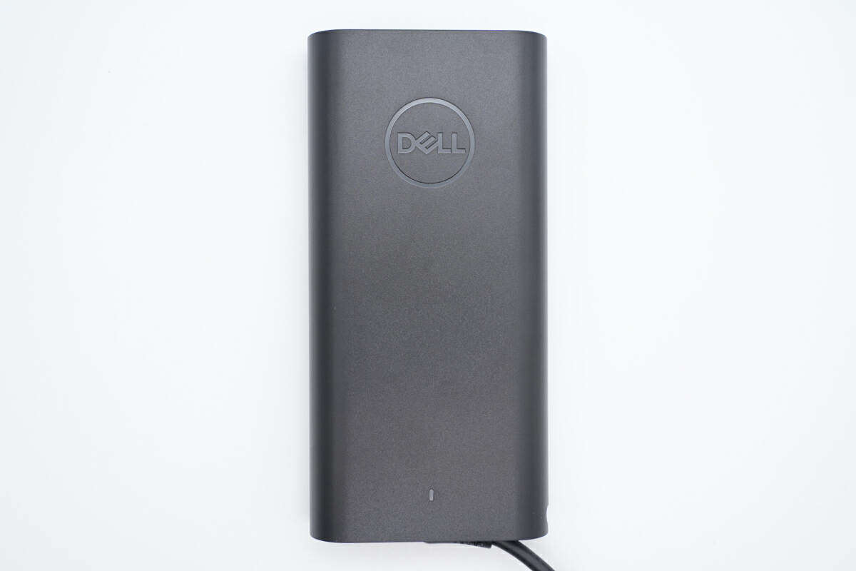
The front of the fuselage is a very classic DELL brand design of Dell power supply, with an indicator light near the edge of the output terminal.

The DELL brand and the outer ring are concave and brightly finished.
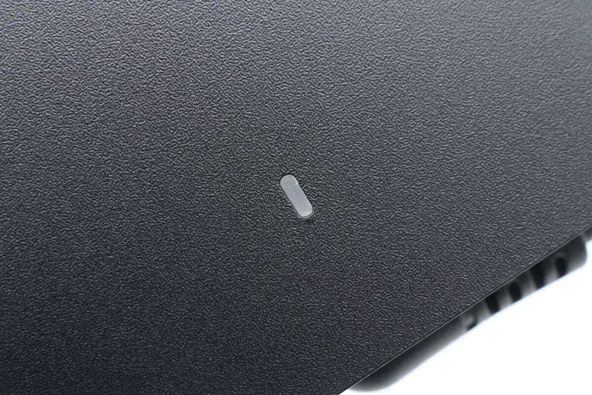
Close-up of indicator light.
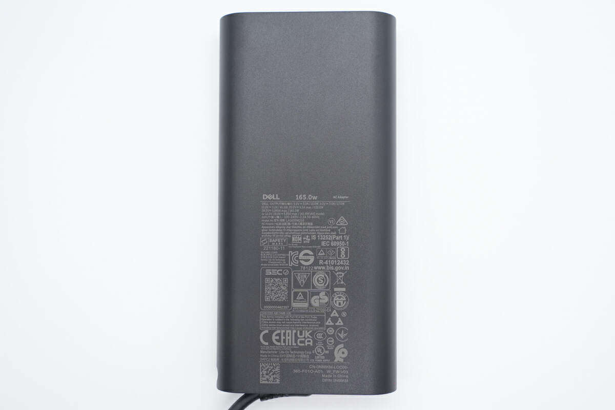
The detailed parameter information of Dell’s gallium nitride power adapter is printed on the back of the fuselage.
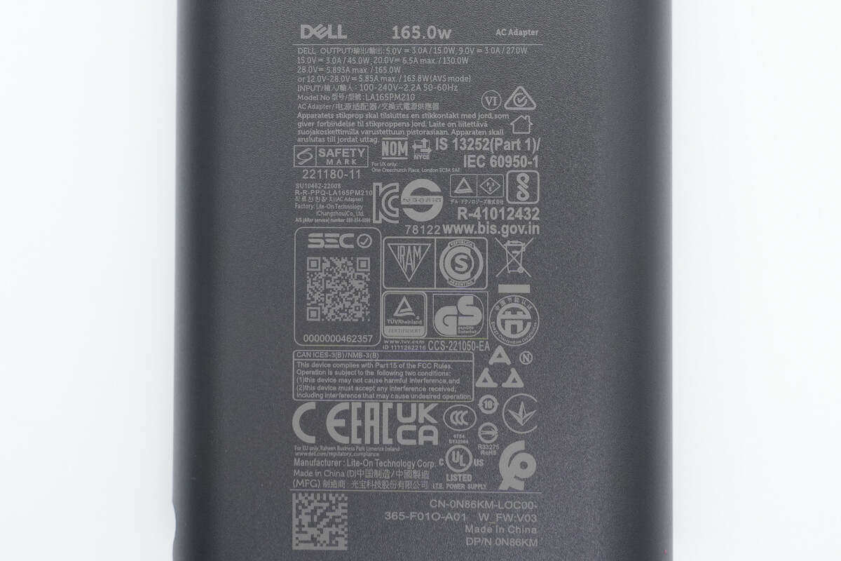
Product parameters close-up
Model: LA165PM210
Input: 100-240V~50/60Hz 2.2A
Output: 5V3A, 9V3A, 15V3A, 20V6.5A, 28V5.893A, 12-28V5.85A
Manufacturer: Lite-On Technology Co., Ltd.
The adapter has passed many certifications such as CCC, CE, EAC, UL, UKCA, CP, GS, KC, PSE, NOM, NYCE, etc. With the separate wire body design, the specification pins can be replaced at any time, and can be used in most countries and regions around the world.
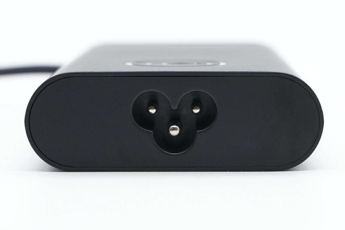
The input end of the fuselage is equipped with a Torx jack.
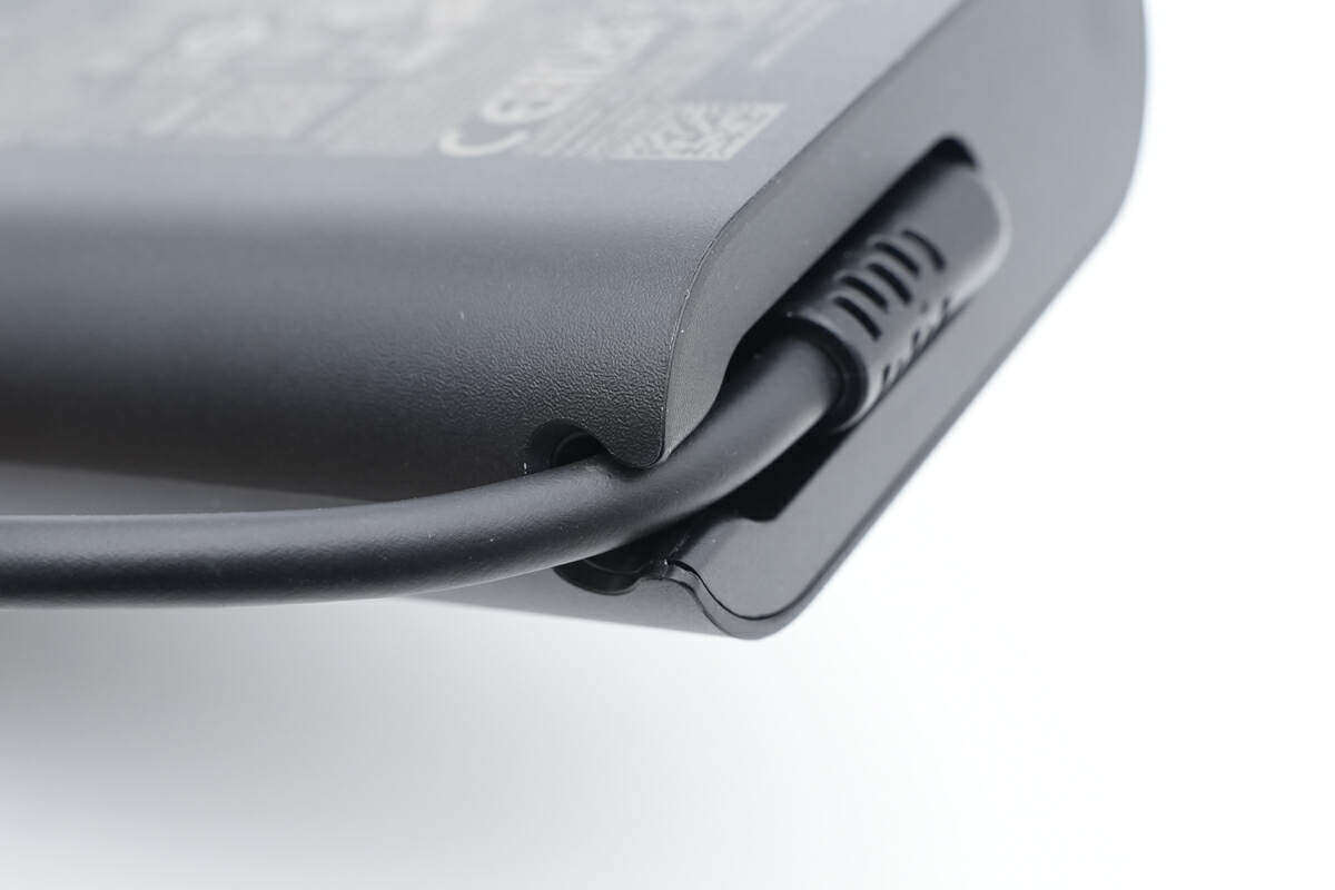
The fuselage is equipped with a lock slot at the output cable to better protect the cable.
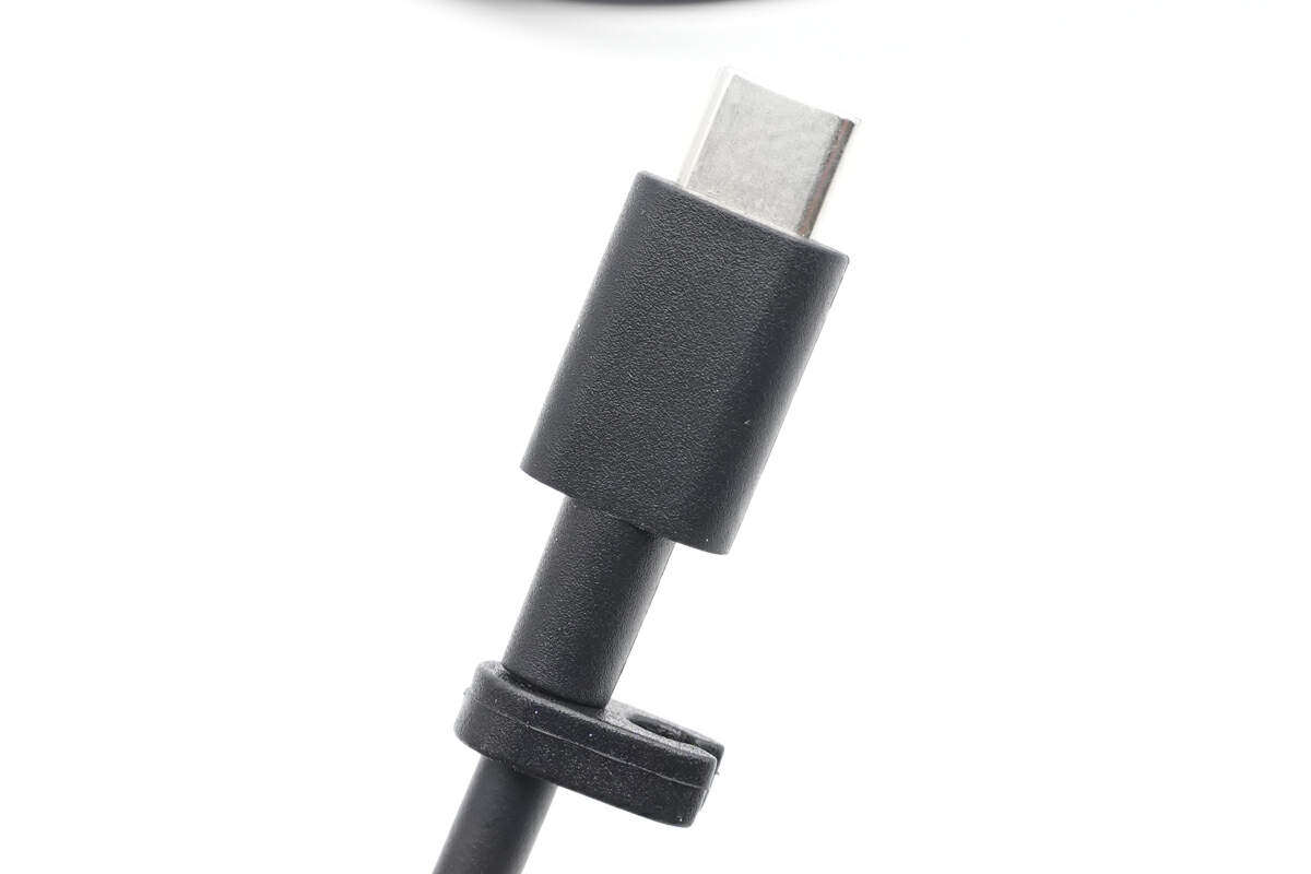
There is a lock at the end of the USB-C cable net to facilitate users to organize the cables, and the design details are in place.
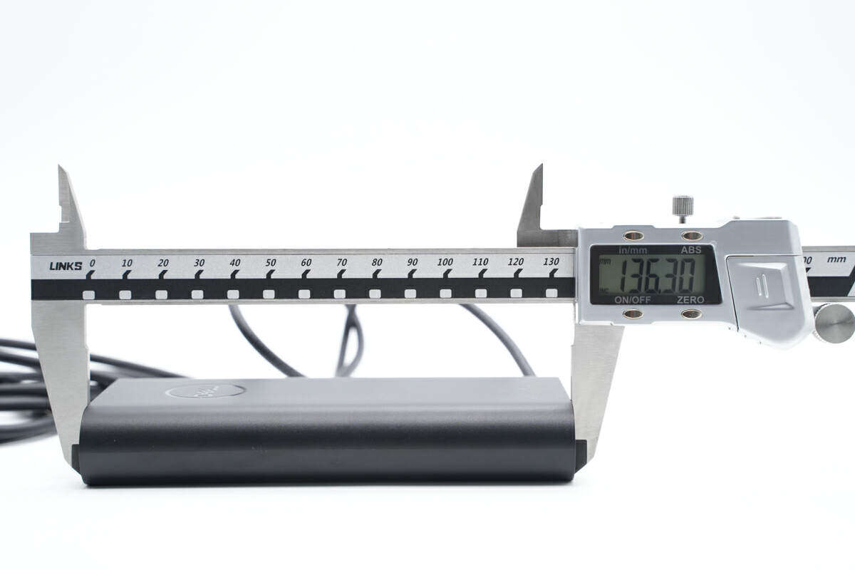
The measured length of this power adapter is 136.3mm.
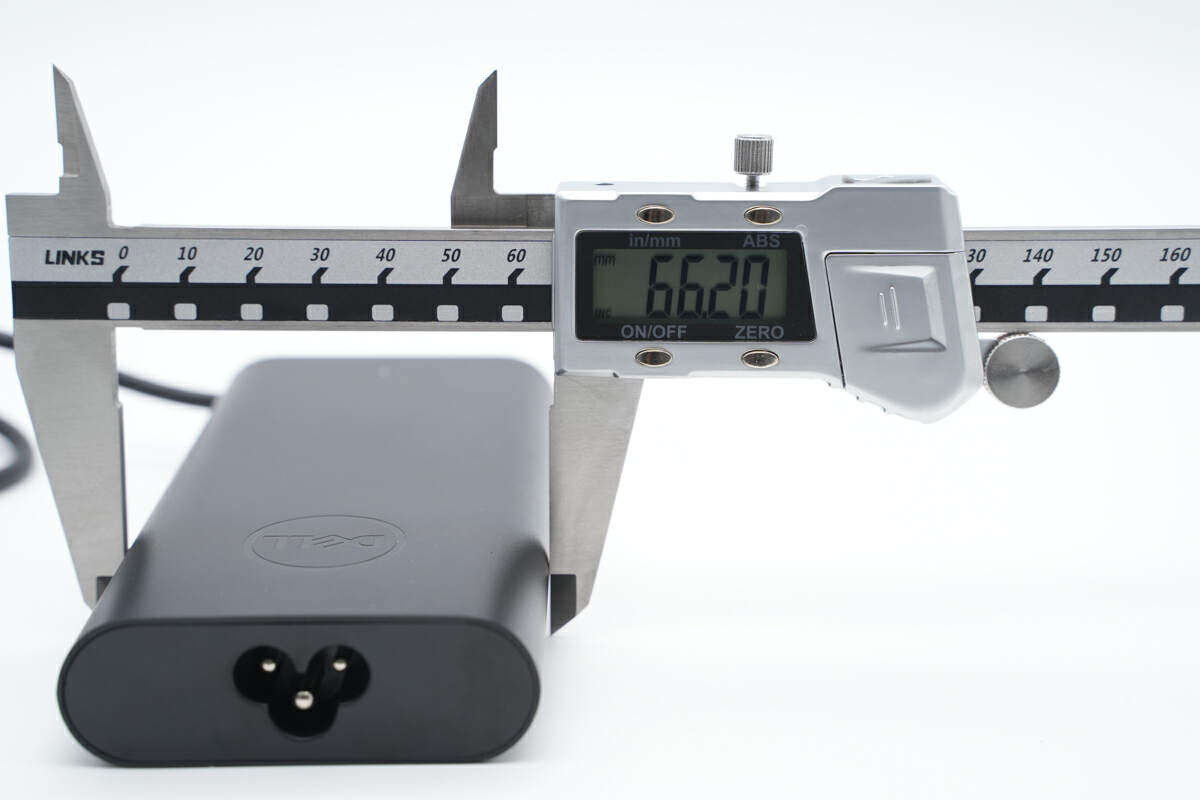
Width is 66.2mm.
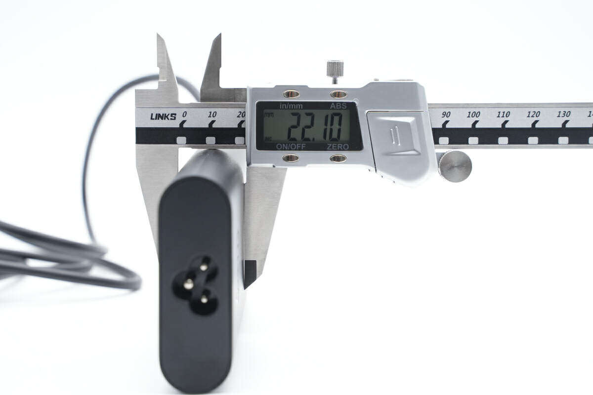
Thickness is 22.1mm.
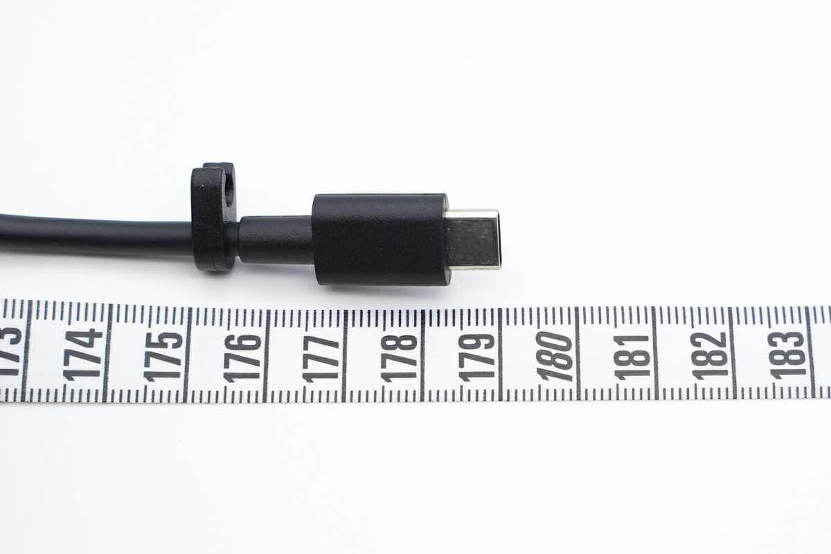
The USB-C cable length is approximately 179cm.
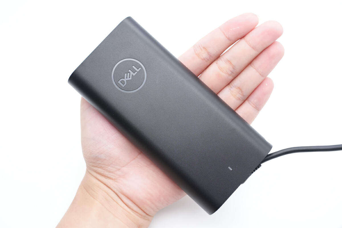
The size of the power adapter body in your hand is intuitive.
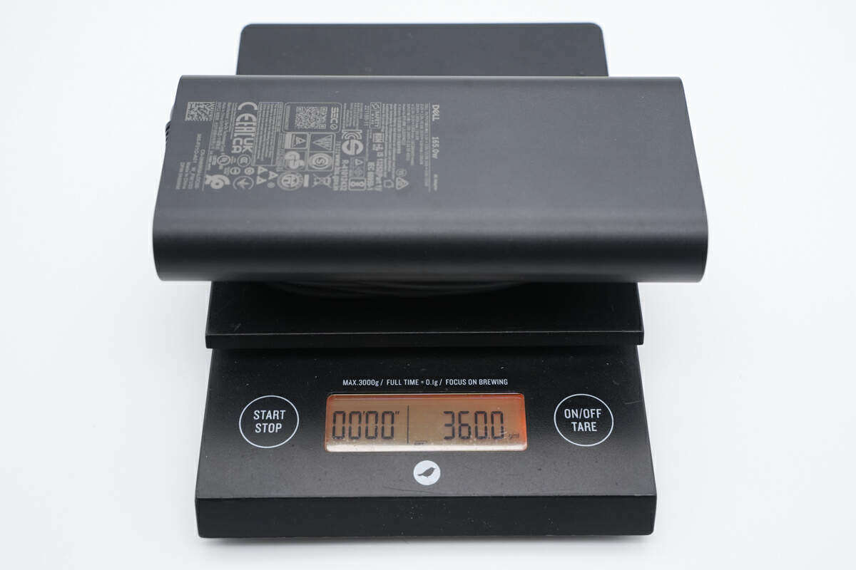
The measured weight of the power adapter body and output cable is 360g.
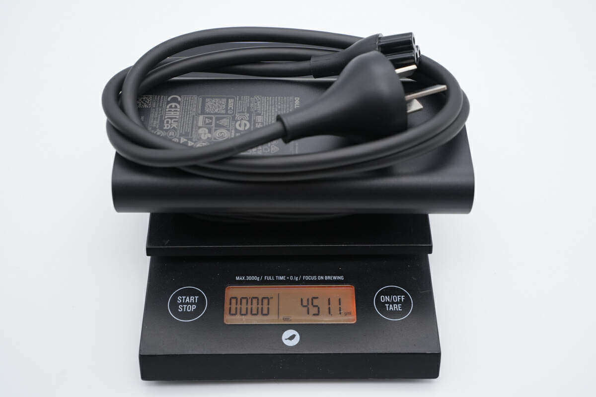
Including the power cord, the total weight is about 451g.
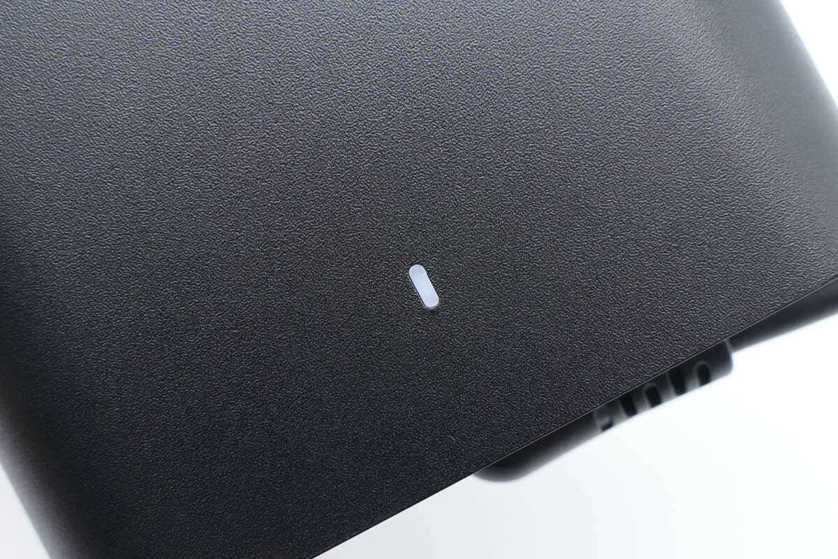
When powered on, the indicator light lights up white.

Using ChargerLAB POWER-Z KM003C, it was measured that the USB-C port supports PD3.1 and DCP charging protocols.
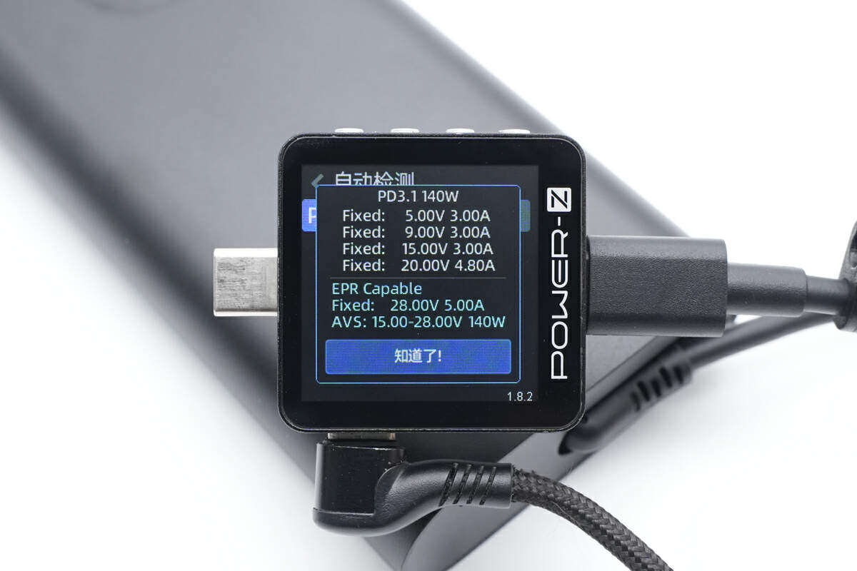
The PDO message shows that the USB-C port has five sets of fixed voltage levels: 5V3A, 9V3A, 15V3A, 20V4.8A, and 28V5A, as well as 15-28V 140W AVS voltage levels.
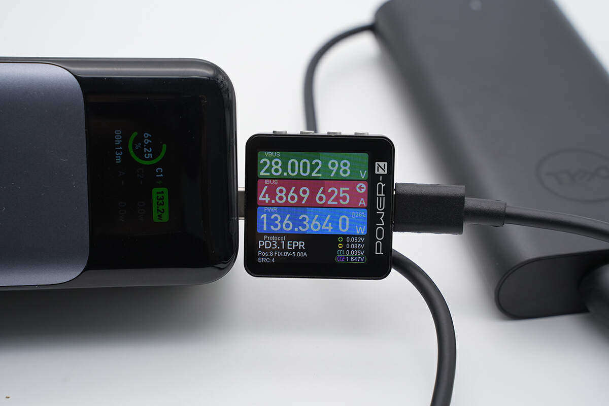
Use Dell’s power adapter to charge the Anker 140W mobile power supply. The measured charging power is 28V 4.87W 136.36W, and USB PD3.1 fast charging is turned on.
Dell 165W GaN power adapter teardown
After looking at the appearance and testing of this power adapter, let’s dismantle it and take a look at the internal solutions and materials.
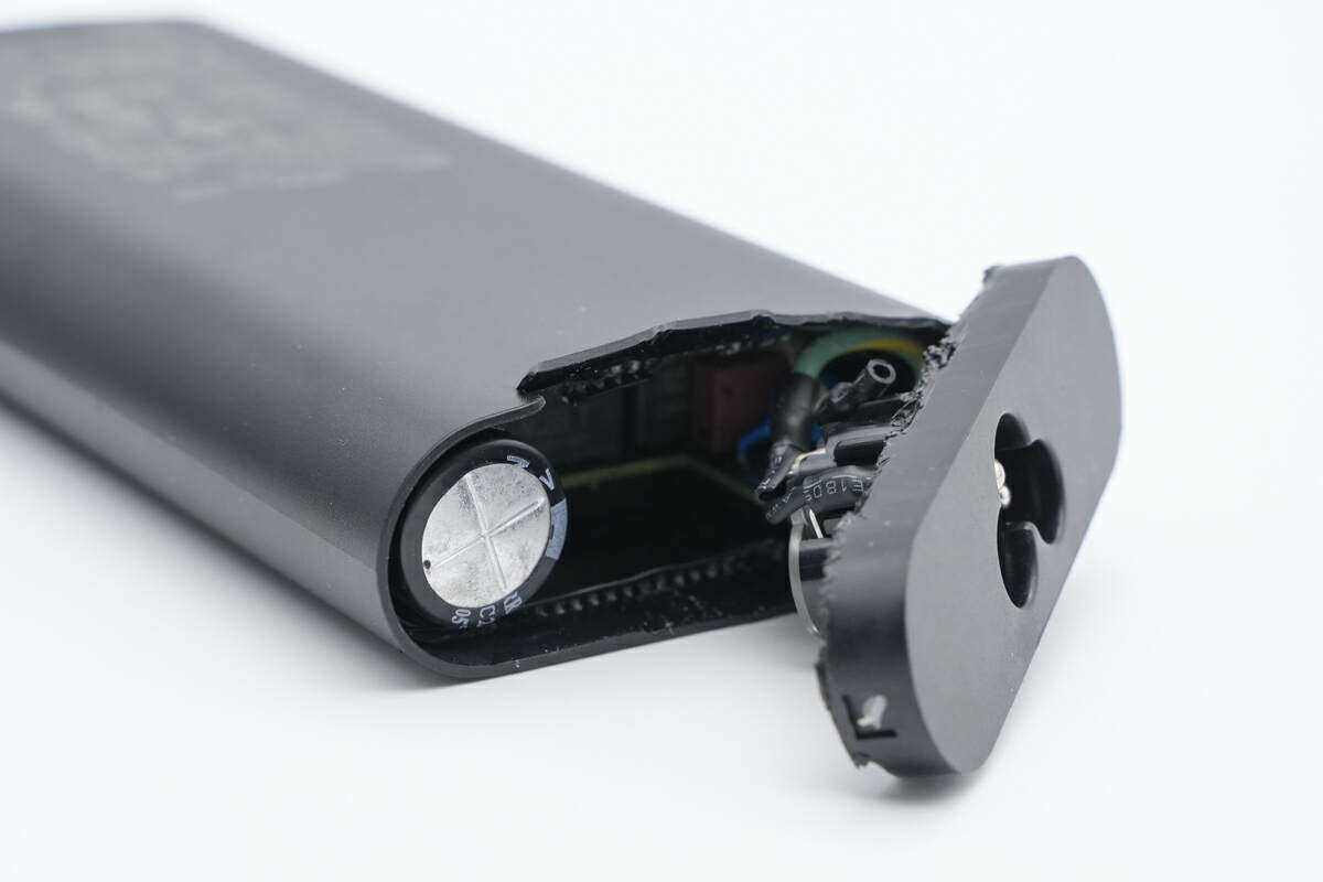
First, pry off the side cover of the power adapter.
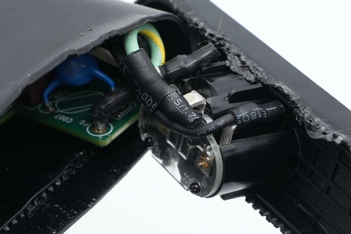
The end cap is ultrasonic welded, the internal socket is insulated by a transparent plastic plate, and the wire solder joints are insulated by heat shrink tubing.
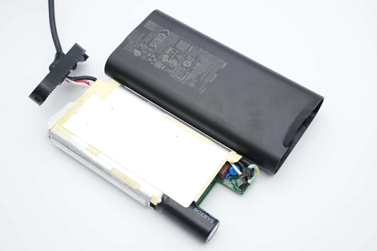
Cut the input wire and pull out the PCBA module from the casing. The PCBA module is wrapped entirely with aluminum sheets for heat dissipation.
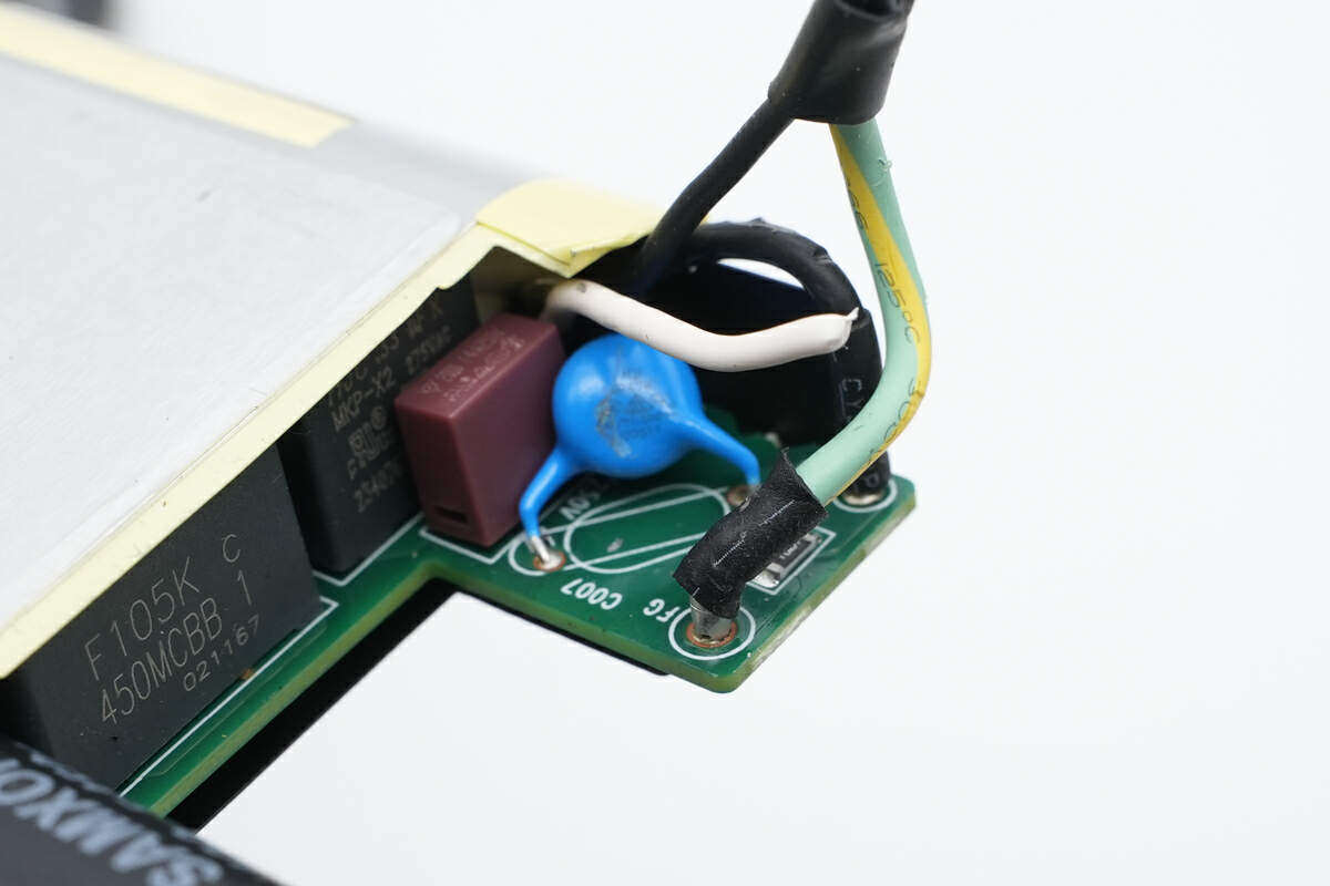
Input wire cold-pressed terminal welding.
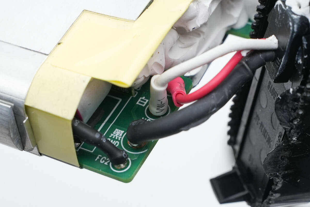
The output wires are also welded with cold-pressed terminals and insulated with heat-shrinkable tubes.
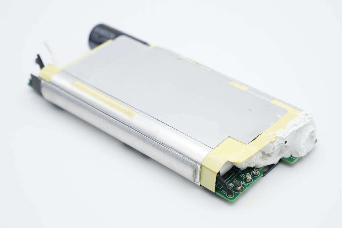
Aluminum sheets are pasted on the side of the PCBA module to fit the shape of the shell and fill the gaps.
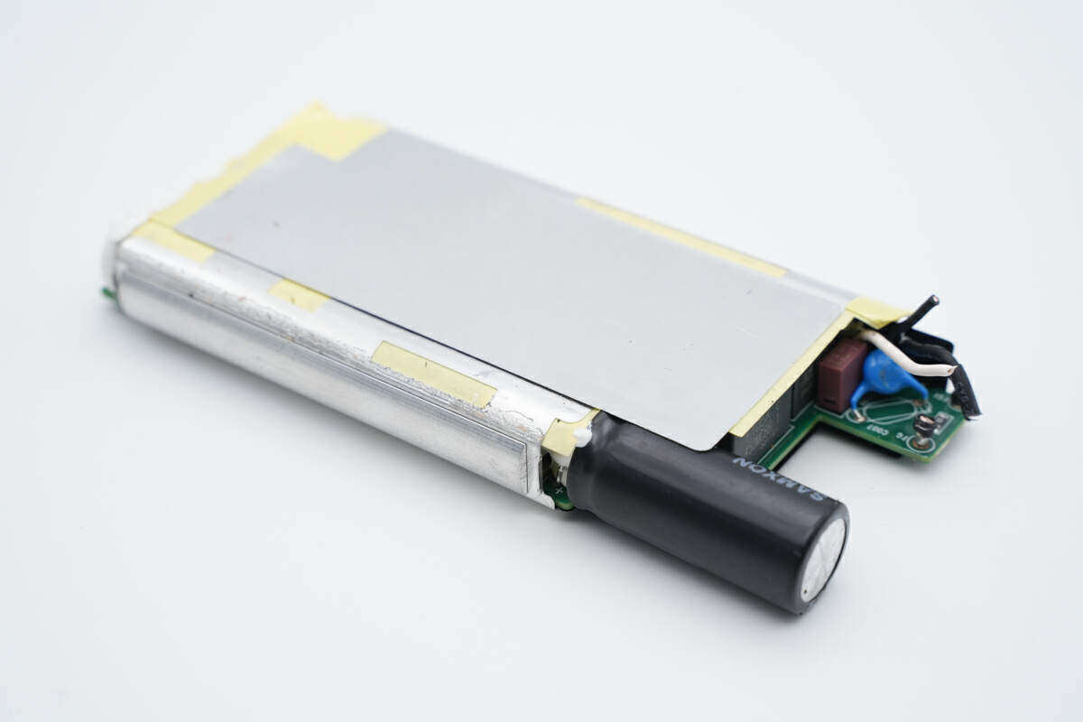
Aluminum sheets are also pasted on the other side to fill the gaps.
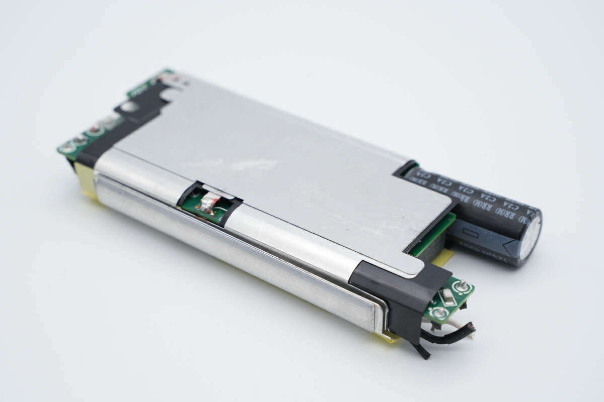
The heat sink is welded and fixed to the back of the PCBA module and insulated by Mylar sheets.
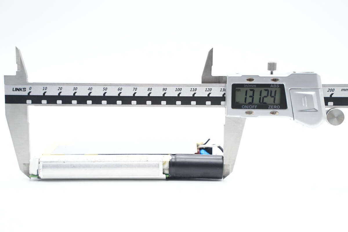
The length of the PCBA module measured using a vernier caliper is approximately 131.2mm.
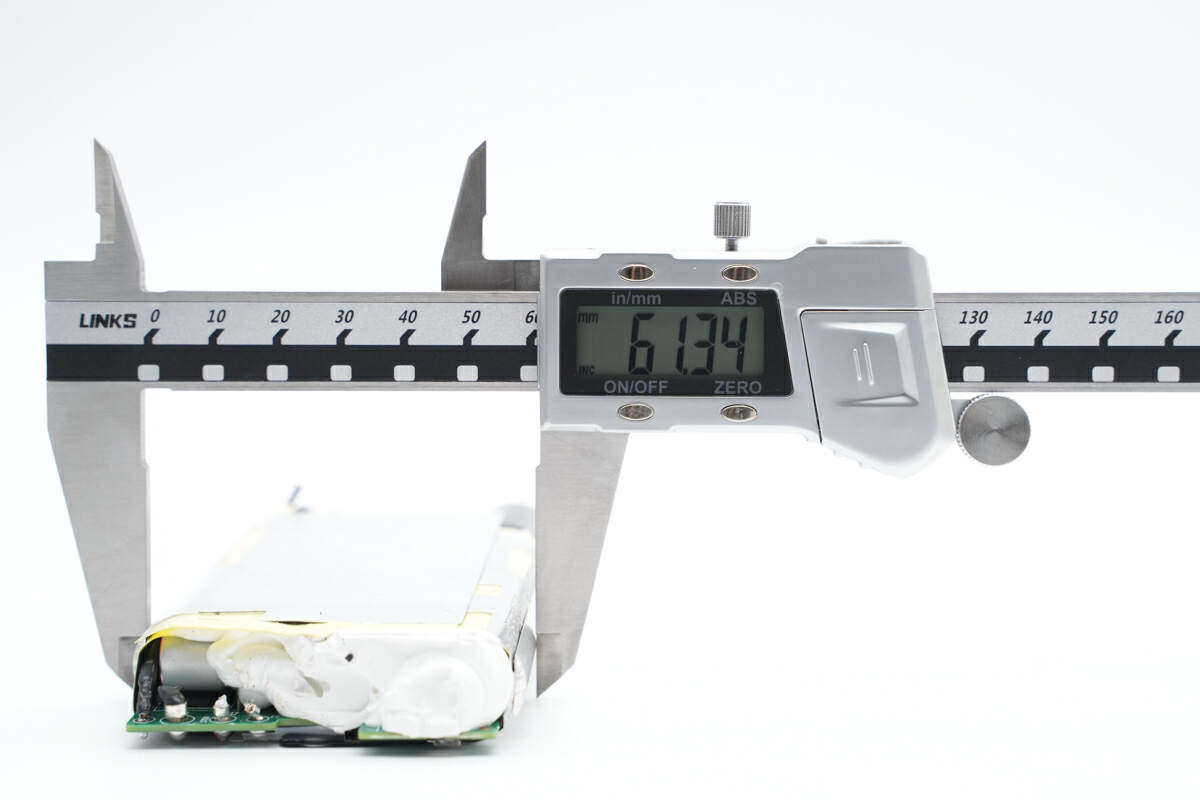
PCBA module width is approximately 61.34mm.
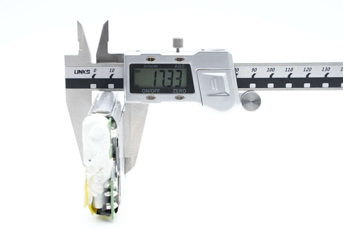
The PCBA module thickness is approximately 17.33mm.
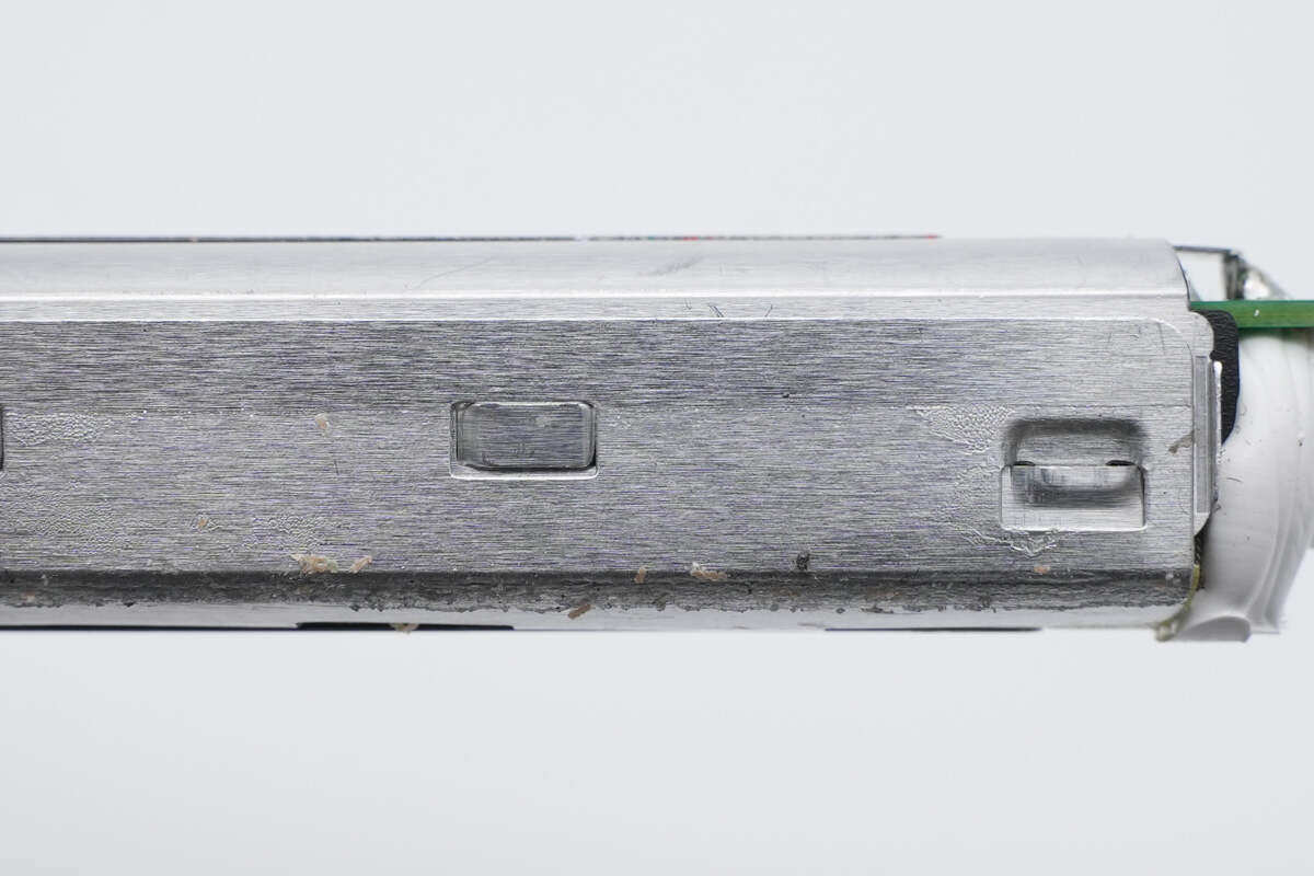
The heat sink is fixed with buckles.
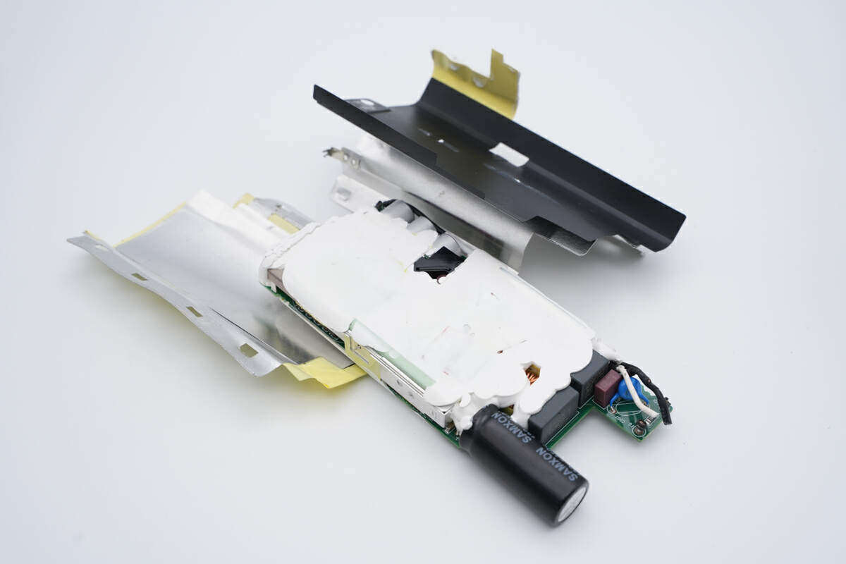
Open the buckle on the side, remove the heat sink, and fill the entire PCBA module with glue.
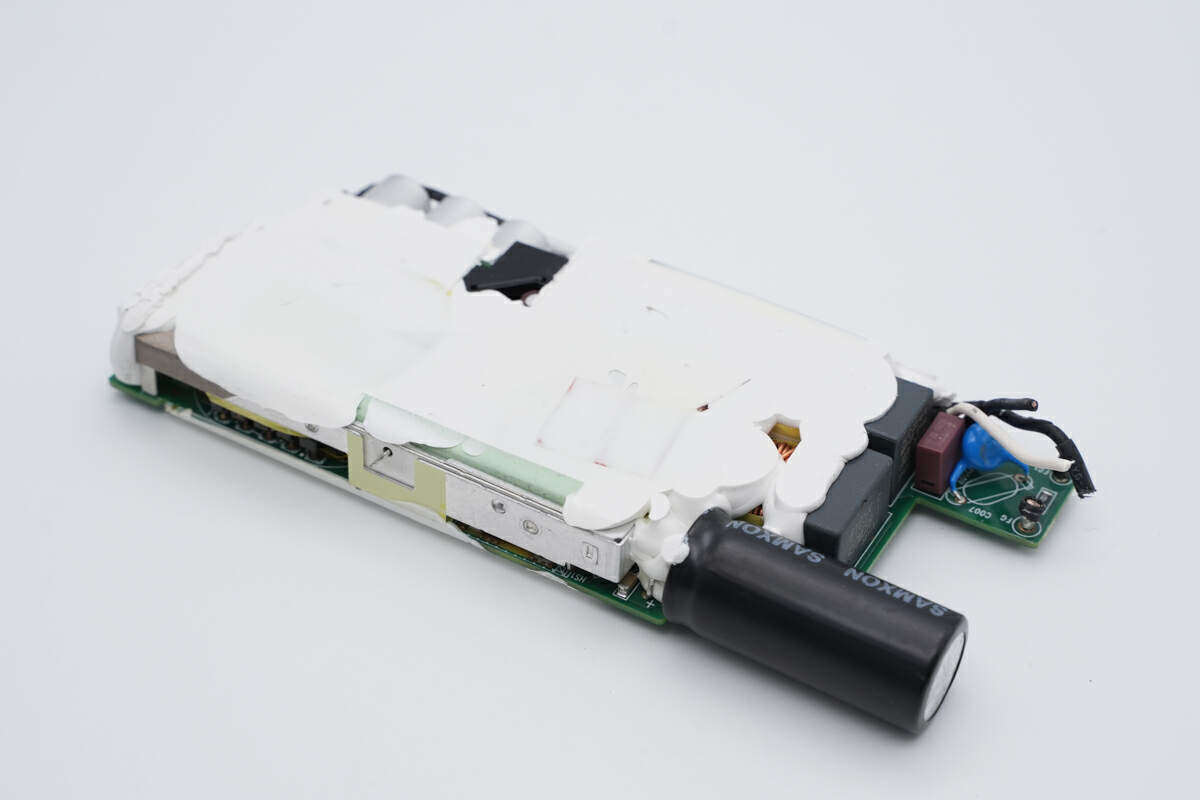
The gaps between the components on the front side of the PCBA module are all filled with thermal conductive glue.
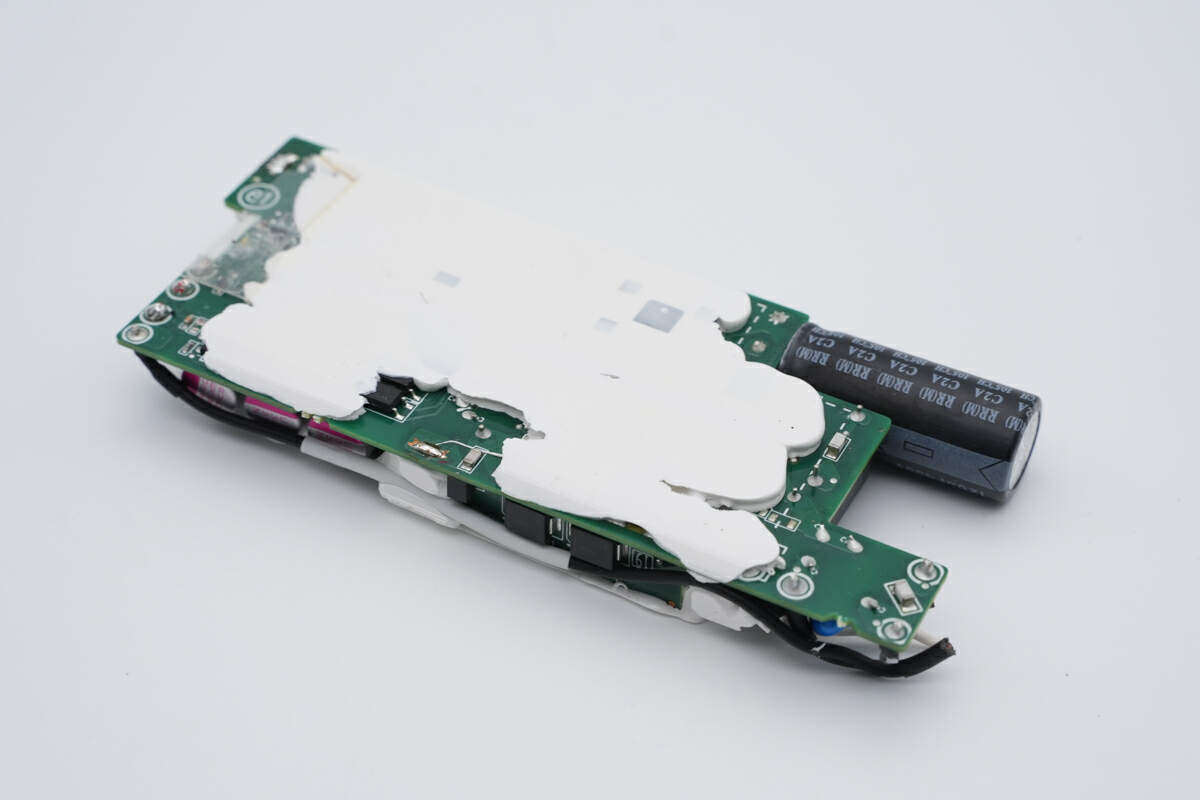
The position corresponding to the heating element on the back is also filled with thermal conductive glue to dissipate heat to the casing heat sink.
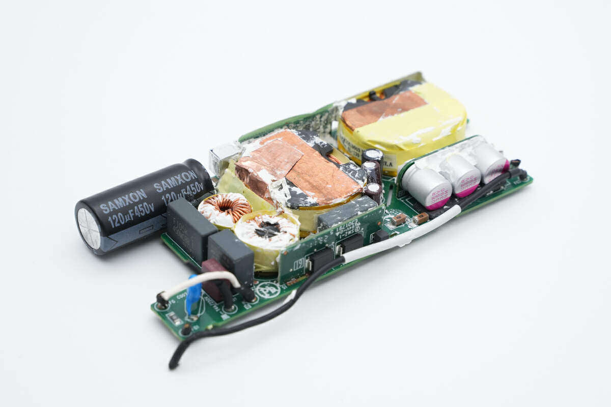
Multiple small boards are welded on the front of the PCBA module to improve space utilization and reduce the overall volume.
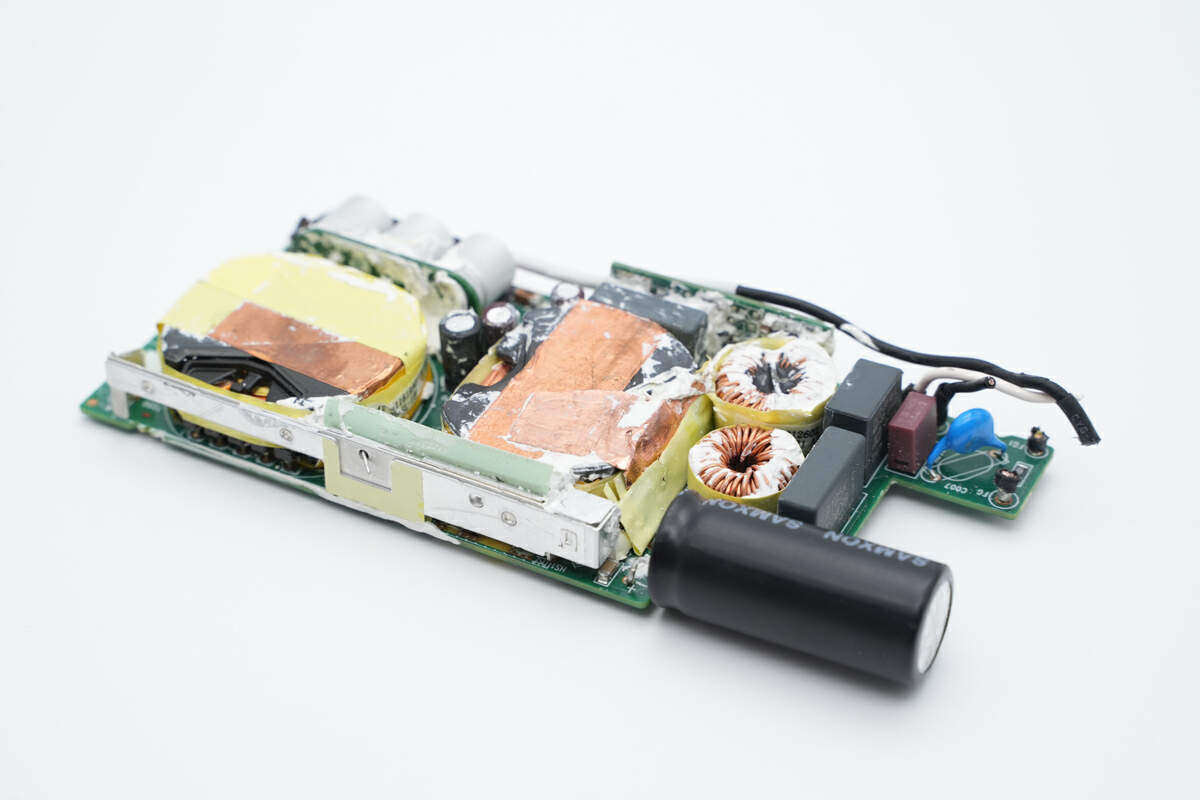
The small plate on the other side has a heat sink fixed on it.
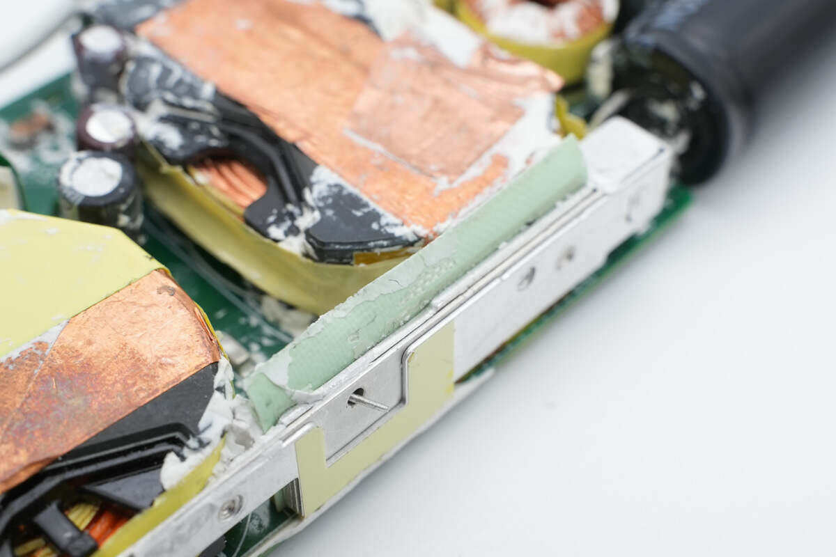
There is a green thermal pad pasted between the small board and the heat sink.
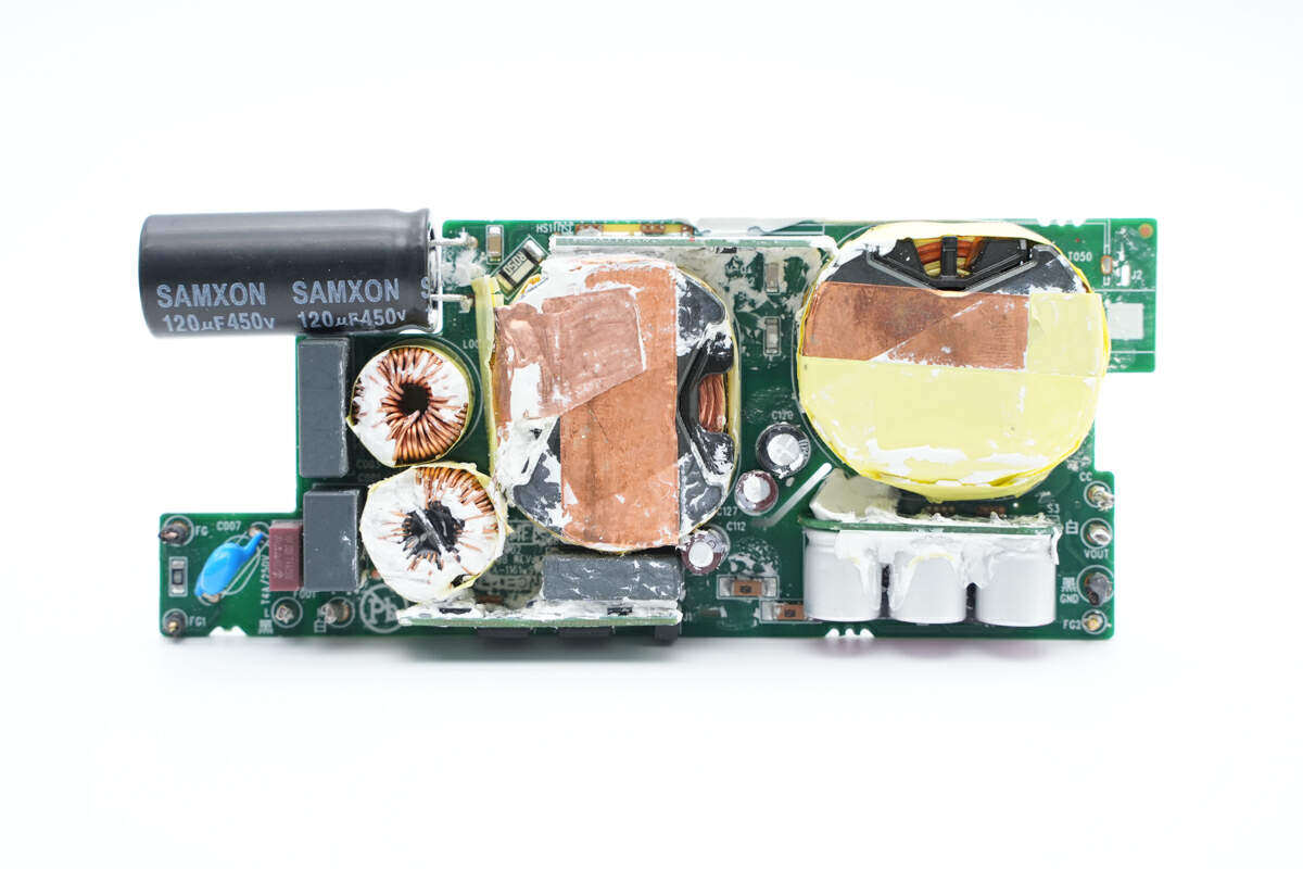
At a glance from the front of the PCBA module, the lower left corner is the AC input terminal, with welded blue Y capacitors, fuses, safety X2 capacitors, and common mode inductors. The small board on the right is the active rectifier circuit. Above are the filter film capacitor and PFC boost inductor. In the upper left corner is the high voltage filter capacitor. The right side is the switching transformer, and the three filter solid capacitors below are welded to the small board to reduce the height.
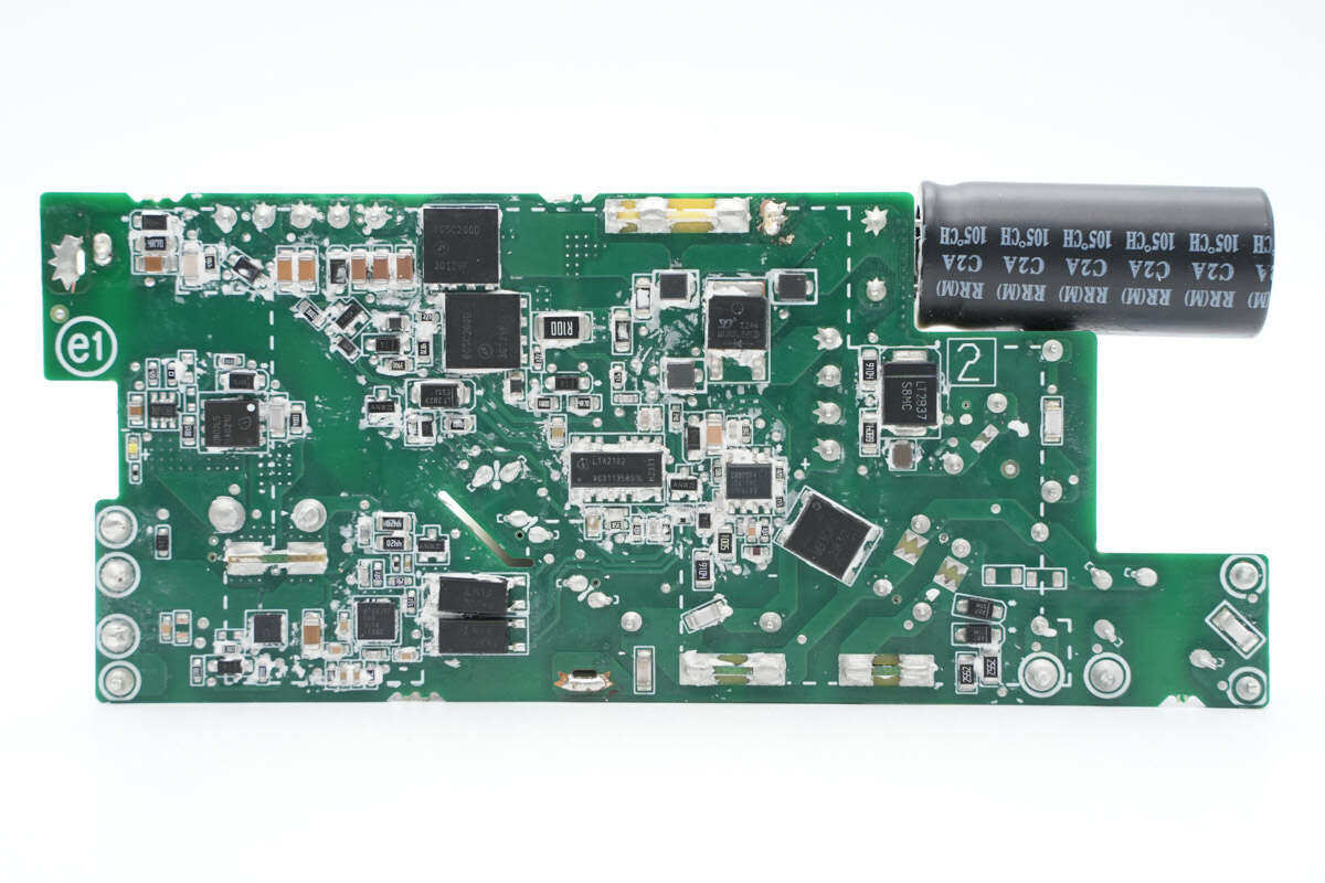
Weld a rectifier bridge, PFC controller, PFC rectifier tube, hybrid flyback controller and half-bridge switch tube on the back. The feedback optocoupler is welded between the primary and secondary, and the synchronous rectification controller, synchronous rectifier tube, protocol chip, VBUS switch tube and feedback optocoupler are welded between the secondary side.
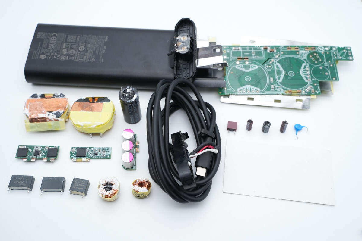
Through observation of the PCBA module, we found that Dell’s laptop power adapter uses active rectification, uses PFC+HFB half-bridge circuit design, synchronous rectification, and wide-range voltage output. Multiple small boards are welded with different functional circuits respectively to improve space utilization and reduce the size of the adapter. Let’s start with the input end to understand the entire charger solution and materials.
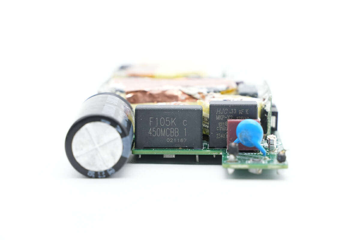
Weld the blue Y capacitor, fuse, safety X2 capacitor and film filter capacitor at the input end of the adapter, and weld the high voltage filter capacitor on the left side.
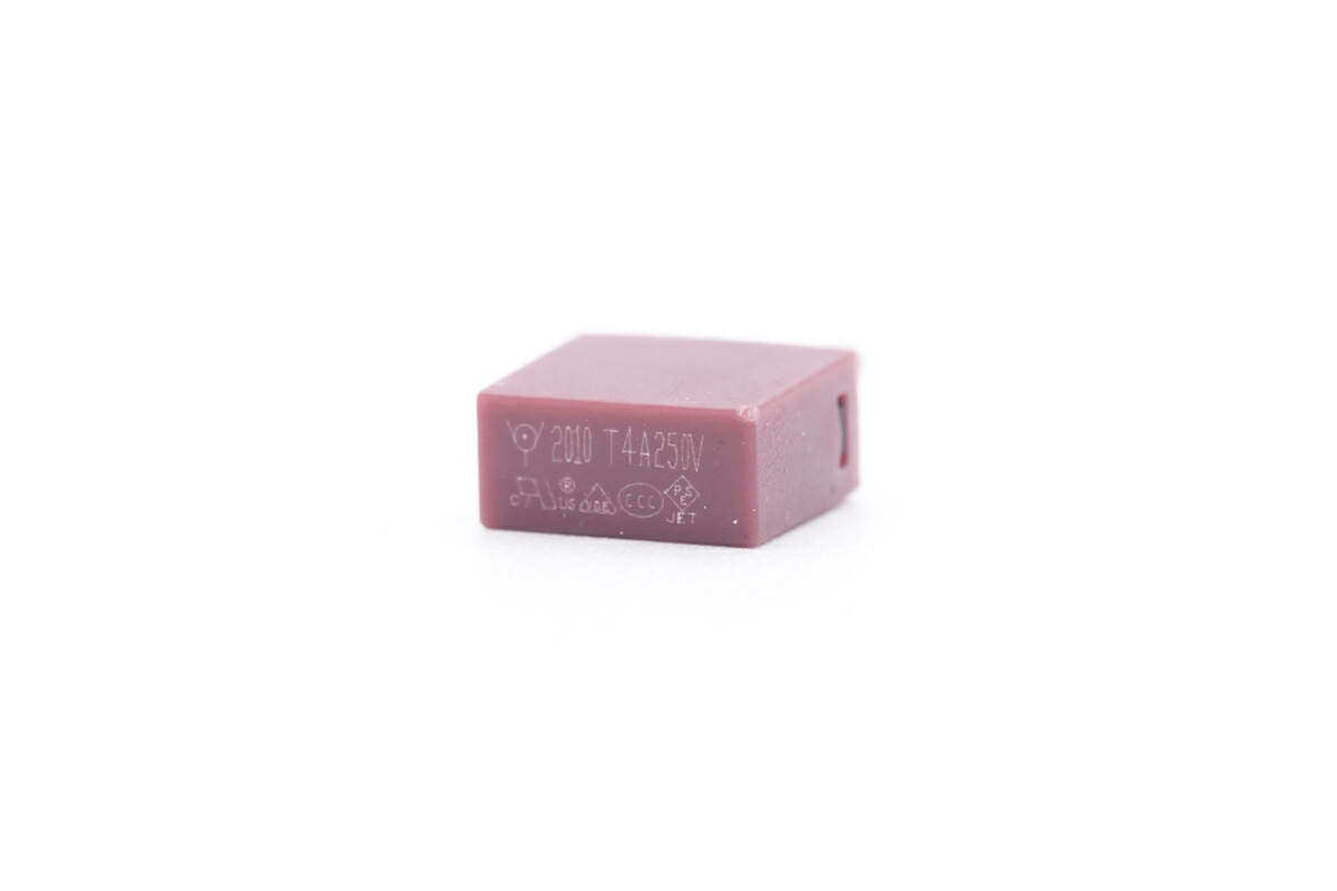
The input fuse is from Huade Electronics, with a specification of 4A 250V.
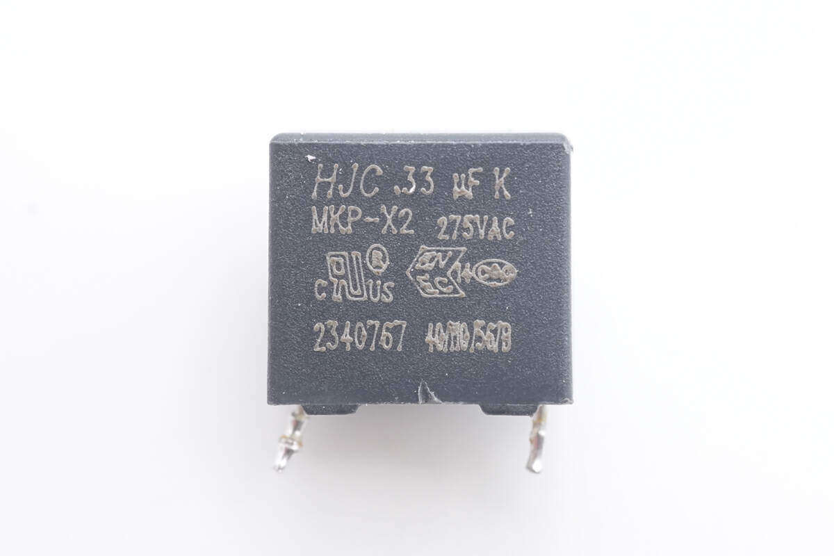
The safety X2 capacitor is from HJC Huarong, with a specification of 0.33μF.
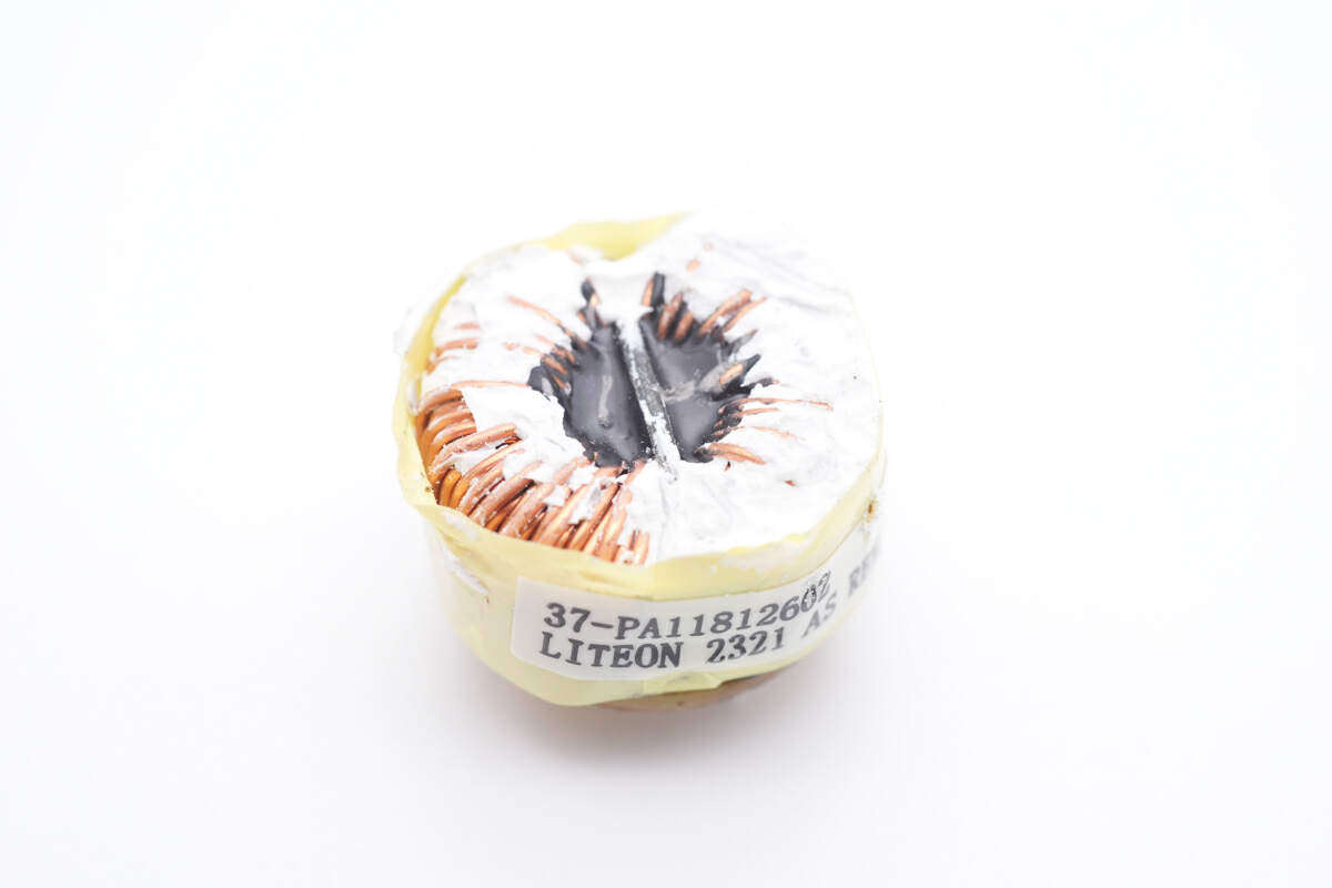
The common mode inductor is wound with enameled wire, and the bottom is insulated by a bakelite board.
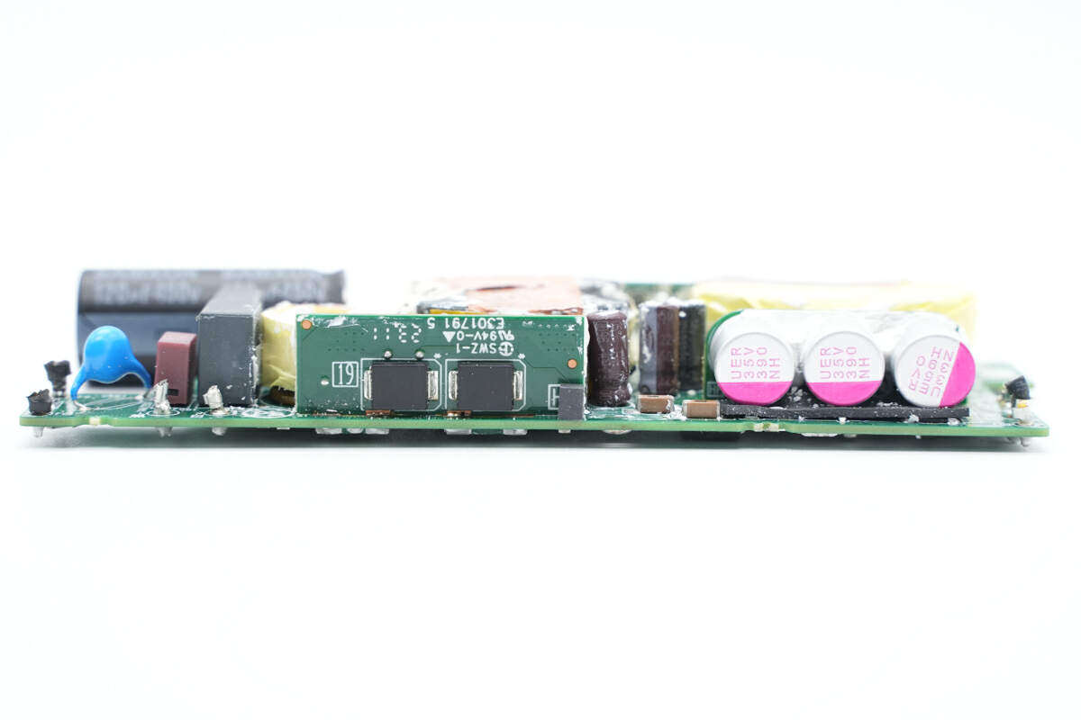
Weld the active rectifier board and filter capacitor board on the side.
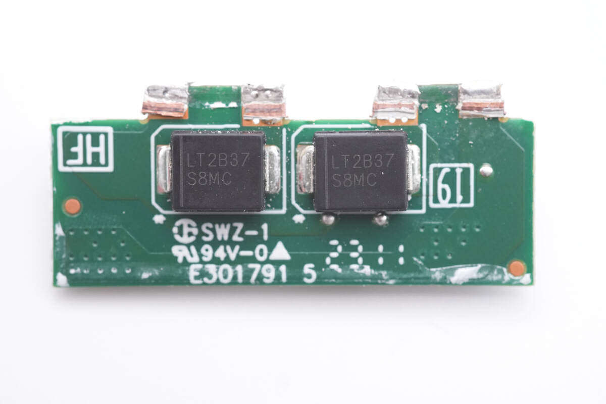
The two rectifier tubes welded on the small board are from Lite-On, model S8MC, specification is 8A 1000V.
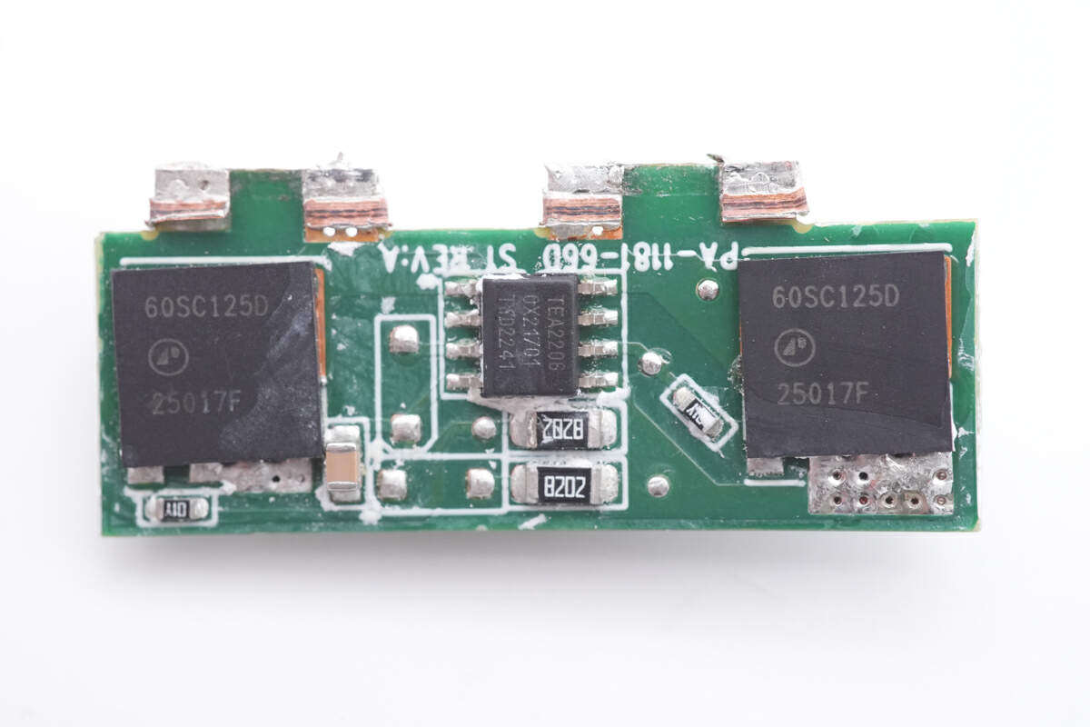
Weld the active rectifier controller and rectifier tube on the other side.
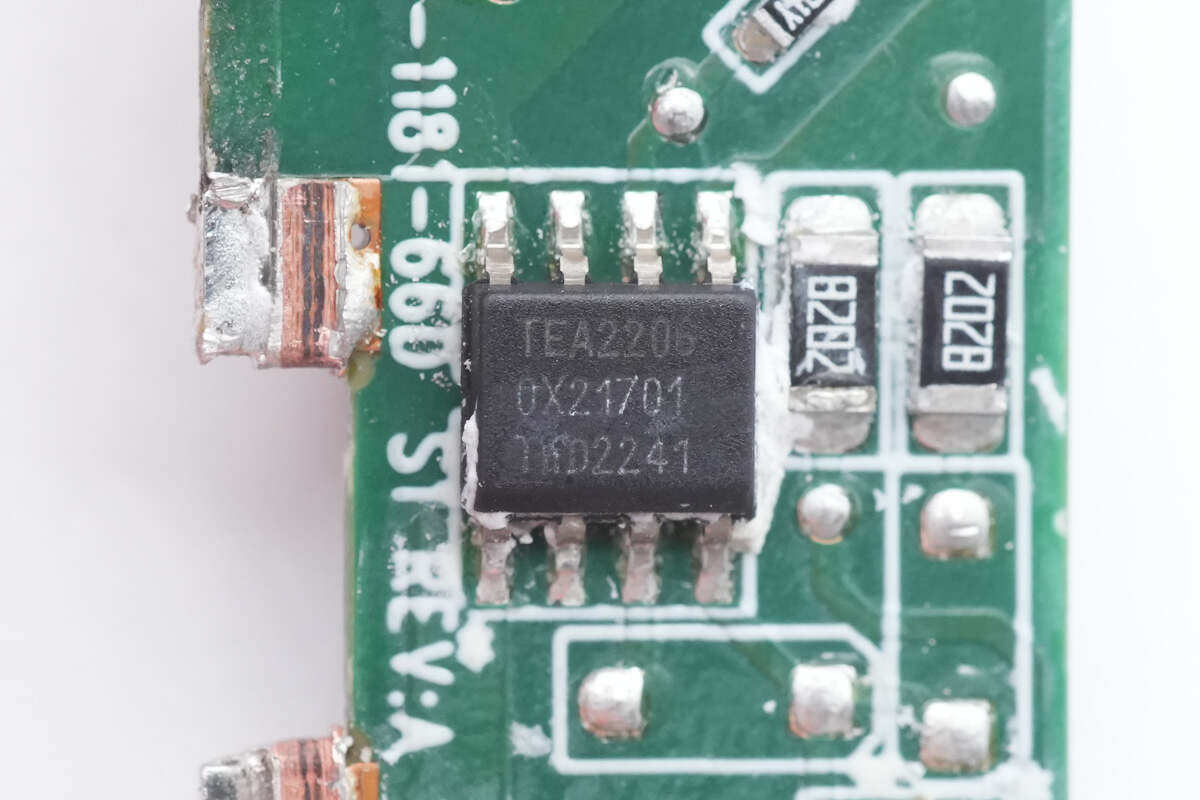
The active rectification control chip is from NXP, model TEA2206. Using two NMOS together, it can reduce the loss caused by the forward voltage drop of the diode and reduce the loss by half. At 90Vac input voltage, the efficiency can be improved by 0.7%. The chip also integrates X2 safety capacitor discharge and self-power supply, and the peripheral components are streamlined.
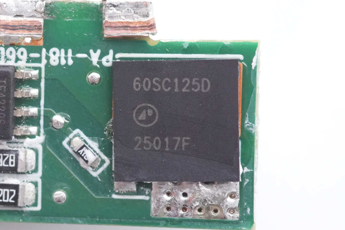
The rectifier is from Fuding Advanced, model AP60SC125DDT8, NMOS, withstand voltage 600V, conductance resistance 125mΩ, and adopts PDFN8*8_HV package.
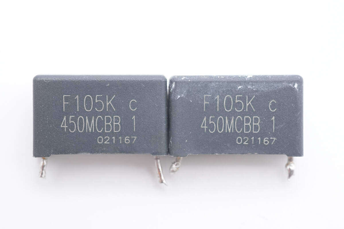
The specifications of the two film capacitors are 1μF 450V.
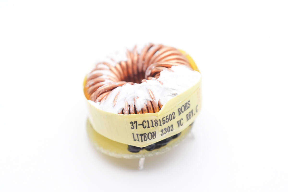
The filter inductor is made of magnetic surround, and the bottom is insulated by bakelite.
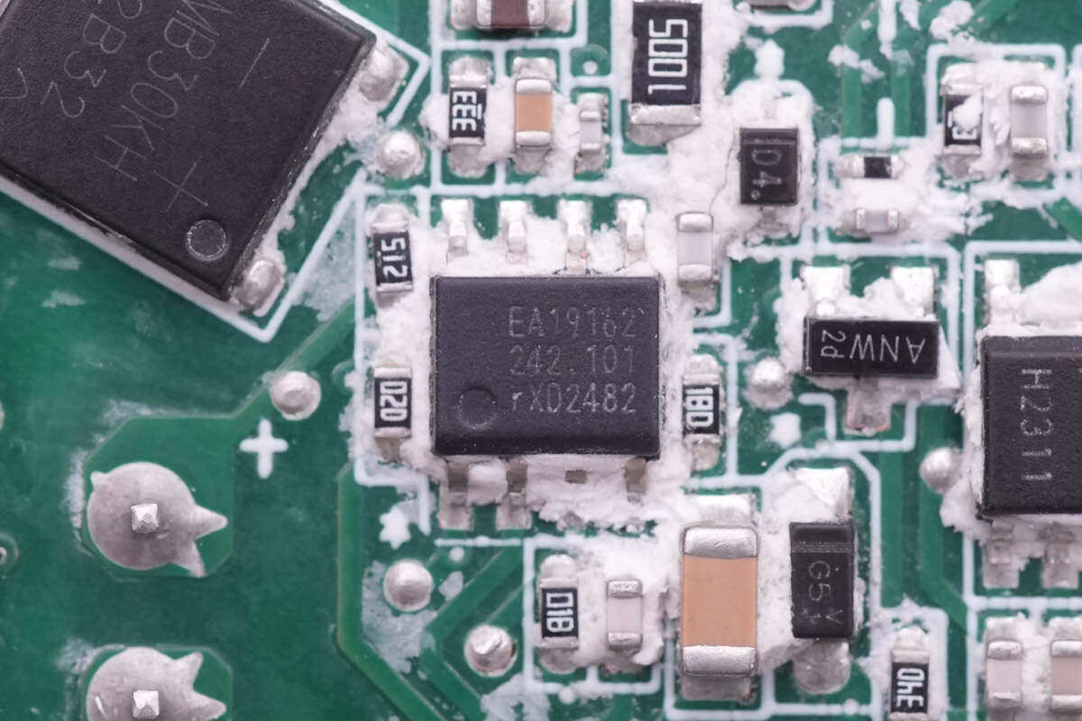
The PFC controller uses NXP NXP TEA19162, which is used to boost the rectified voltage and perform active power factor correction. It integrates X capacitor discharge components internally without external components. It integrates soft start and shutdown and supports high-precision voltage stabilization and boosting. , and has multiple built-in complete protection functions.
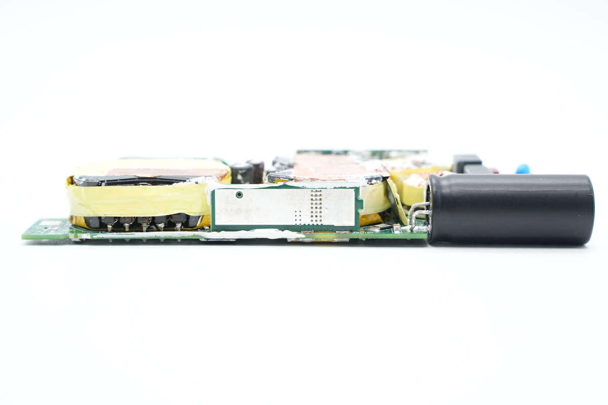
The PFC switch tube is welded on the side of the PCBA module, and the high-voltage filter capacitor is welded on the right side.
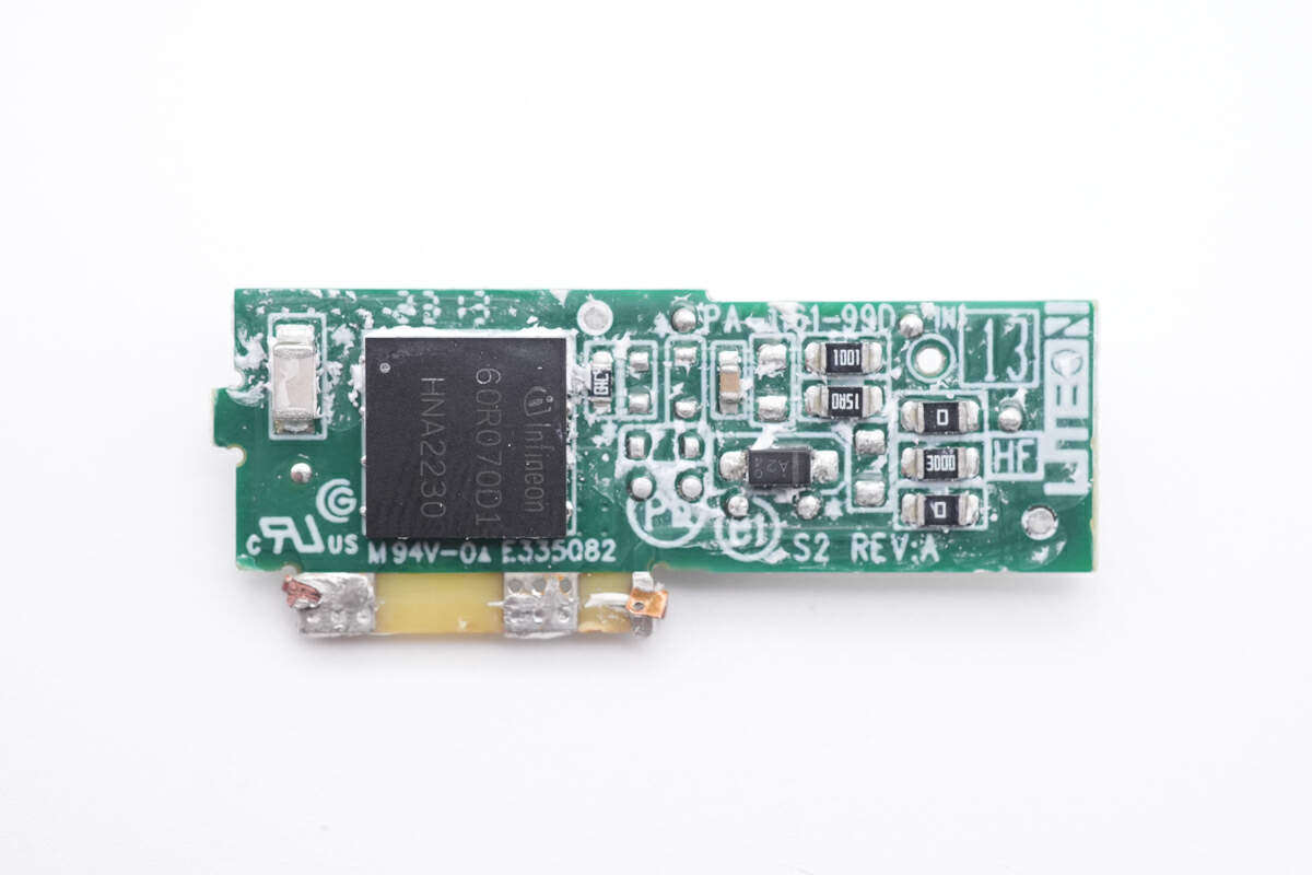
The small side plate is welded to the PFC switch tube.
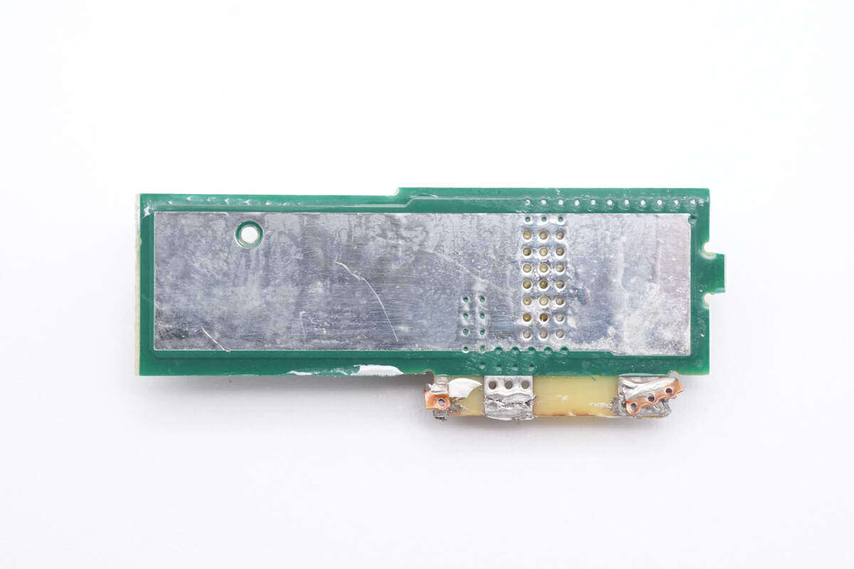
The vias on the back of the board are exposed with copper and tin to enhance heat dissipation performance.
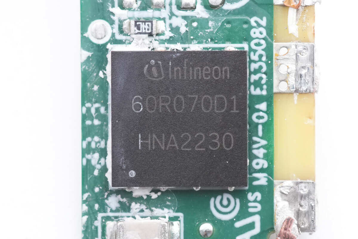
The PFC switch tube is from Infineon, model IGLD60R070D1. It is an enhanced gallium nitride switch tube with a voltage resistance of 600V, a conduction resistance of 70mΩ, and a PG-LSON-8-1 package. Supports industrial, telecom and data center switching power supply applications, supports hard switching and soft switching half bridges, supports totem pole PFC and high frequency LLC applications.
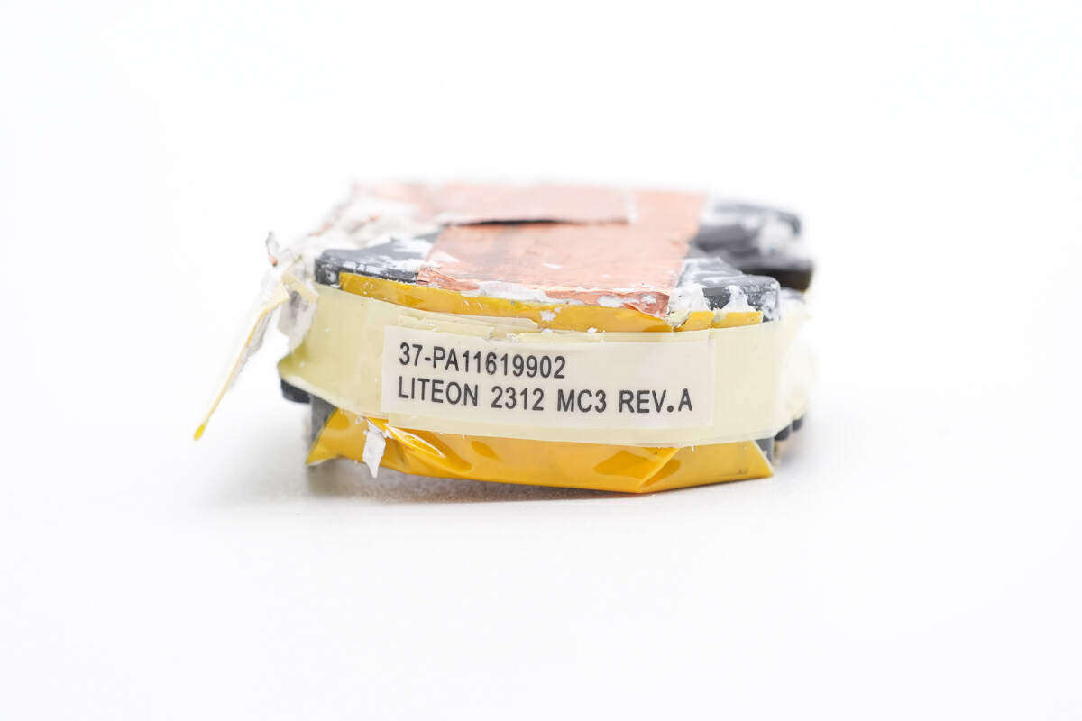
A close-up of the PFC boost inductor, the core is wrapped with copper foil for shielding.
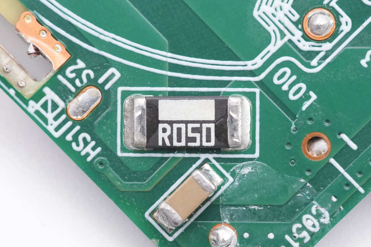
The 50mΩ resistor is used to detect the PFC switch current.
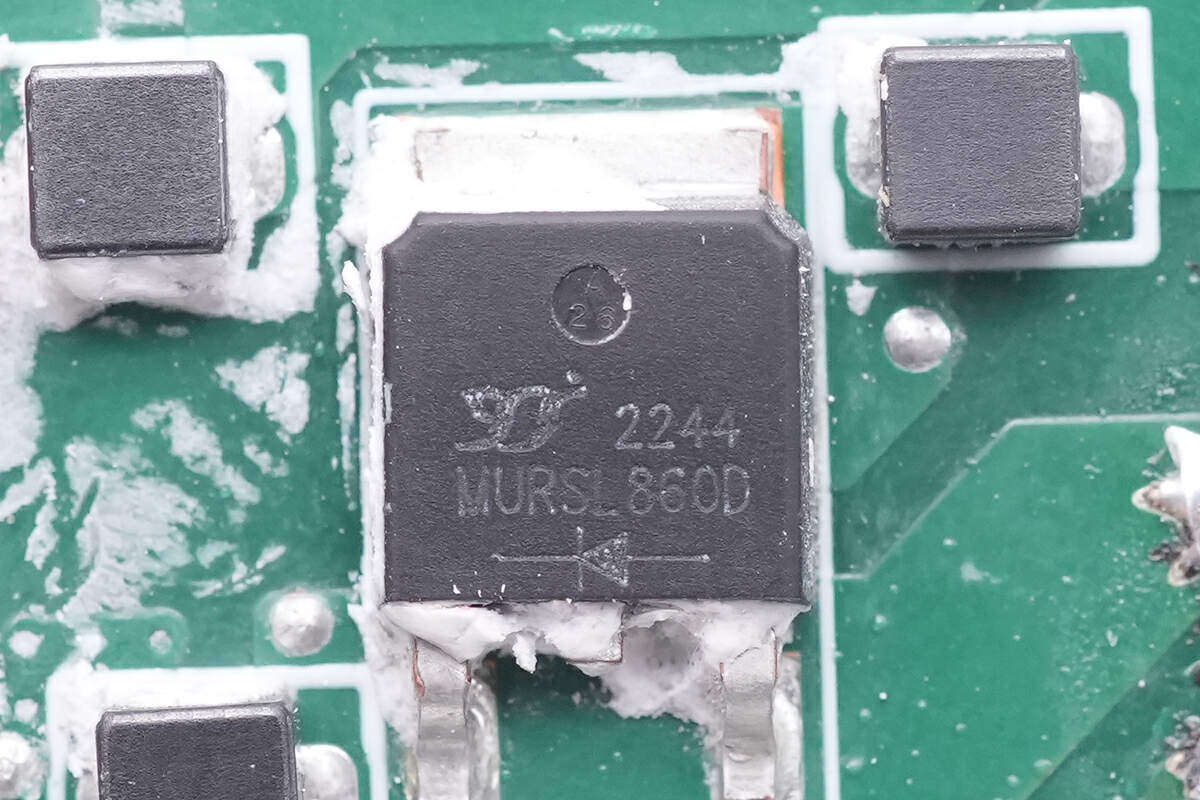
The PFC rectifier is from Yangjie Electronics, model MURSL860D. It is an ultra-fast recovery diode with 8A current and 600V voltage resistance, and is packaged in TO252.

The high-voltage filter capacitor comes from Wanyu, and the specification is 120μF450V.
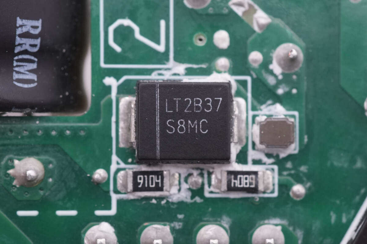
S8MC diodes are used for PFC bypass to charge the high voltage capacitor when the power supply is turned on.
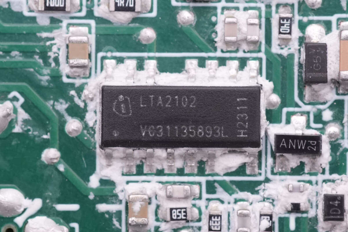
The power supply main control chip is from Infineon, silk-screened LTA2102, and is a customized model.
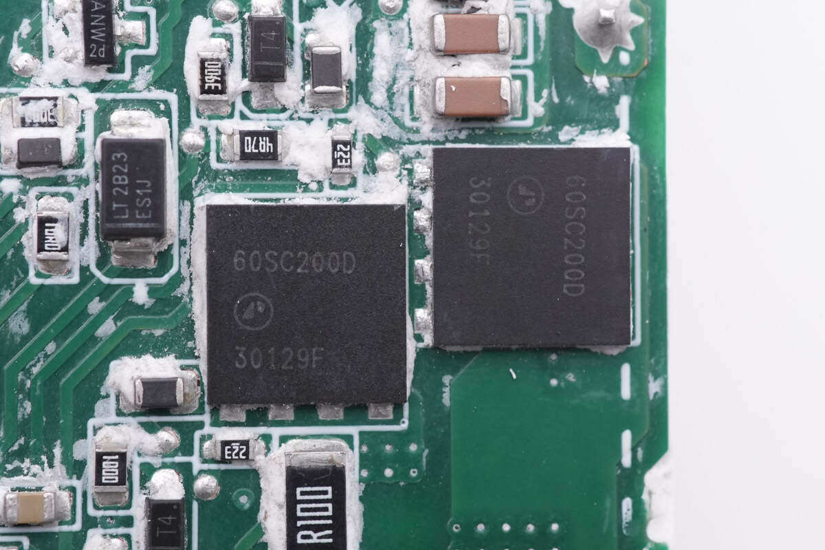
The two half-bridge switch tubes are from Fuding Advanced, model AP60SC200DDT8, NMOS, withstand voltage 600V, conductance resistance 200mΩ, and are packaged in PDFN8*8_HV.
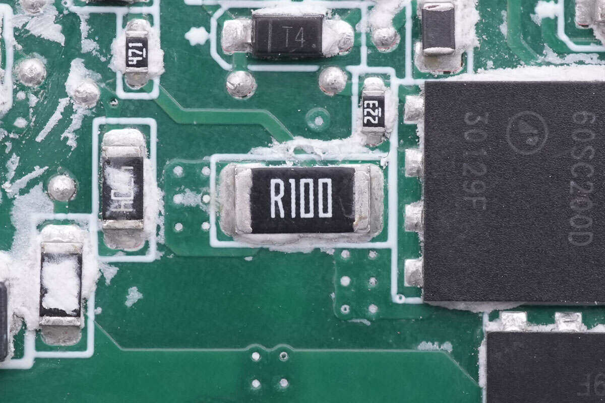
The 100mΩ resistor is used to detect the switch current.
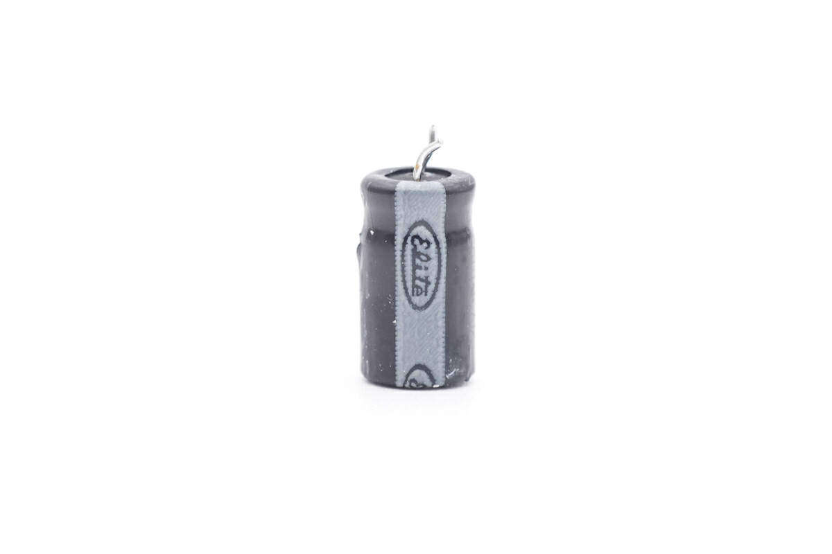
The filter capacitor that supplies power to the main control chip comes from ELITE Jinshan.
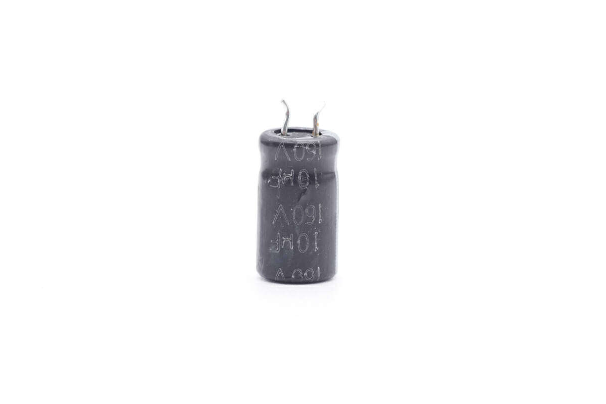
One of the specifications is 10μF 160V.
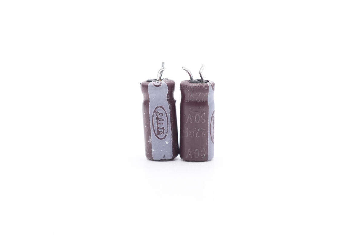
The specifications of the other two filter capacitors are 22μF 50V.
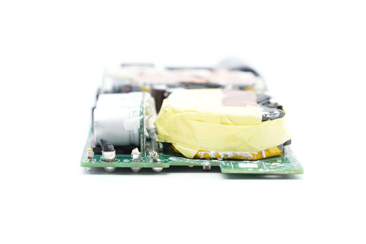
Weld the filter capacitor plate and transformer on the output side.
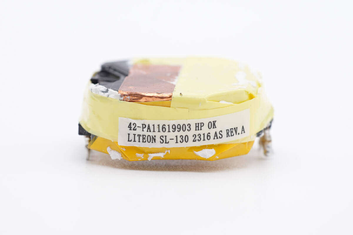
The transformer core is wrapped with copper foil for shielding.

Close-up of blue Y capacitor.
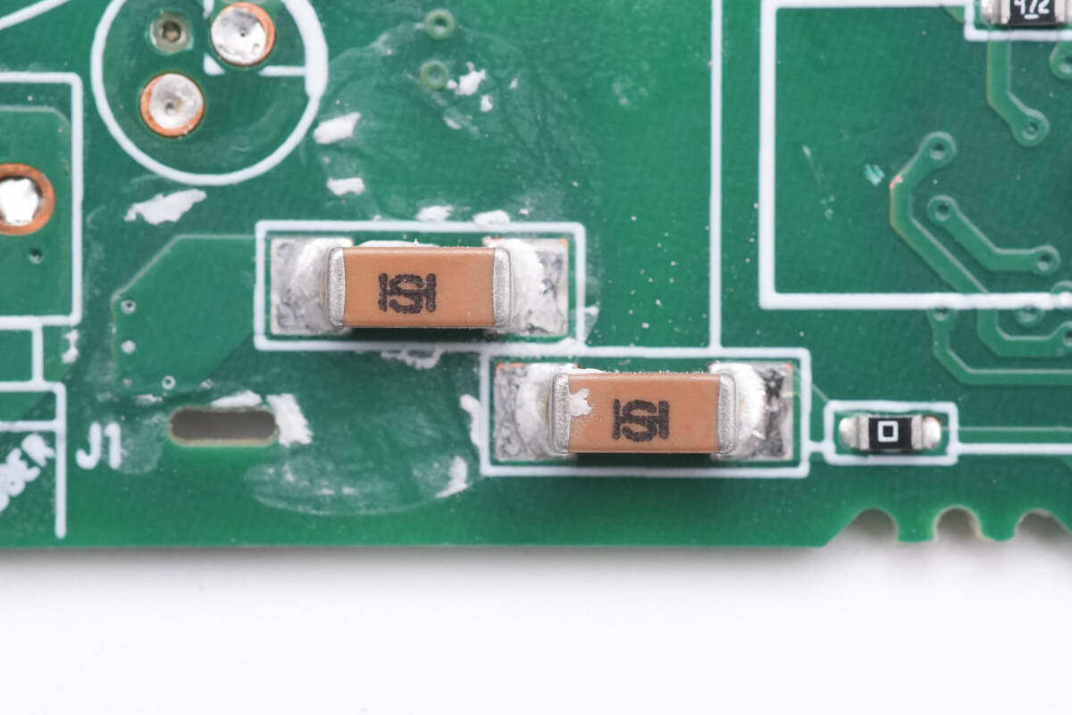
The chip Y capacitors are from He Shentang. Two of them are connected in series to increase the voltage level.
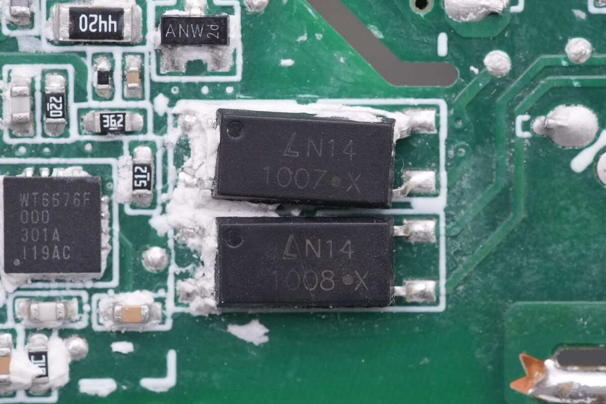
LTV1007 and LTV1008 optocouplers are used for output voltage feedback and PFC control respectively.
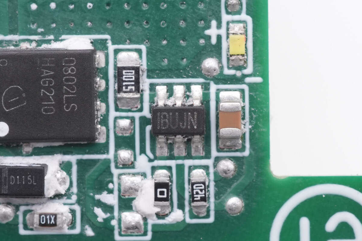
The synchronous rectification controller comes from MPS, silk screen IBUJN, the actual model is MP6951, which is the latest synchronous rectification controller launched by MPS. It supports DCM, CCM, QR, ZVS working modes, and also supports ACF active clamp flyback and HFB hybrid flyback. Excitation, the operating frequency can reach 1MHz, supports driving GaN synchronous rectifiers, supports high-side and low-side applications, and is packaged in TSOT23-6.
The synchronous rectifier is from Infineon, screen printed 0802LS, the actual model is BSC0802LS, it is an NMOS with a voltage of 100V, a conduction resistance of 3.4mΩ, and is packaged in PG-TDSON-8.

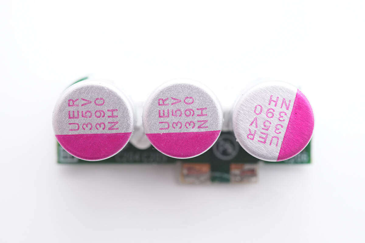
The output filter capacitor is from Wanyu. It is a UER series conductive polymer aluminum solid capacitor with a lifespan of 5000 hours and a specification of 35V 390μF.
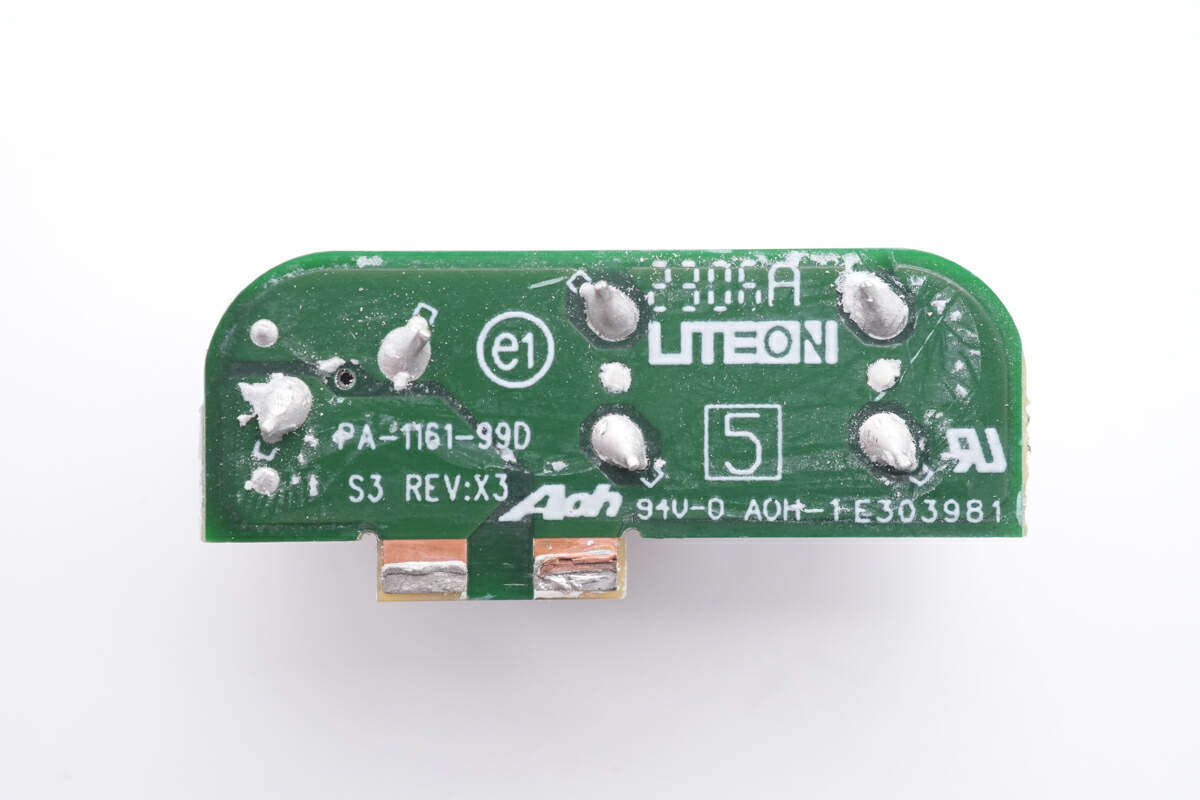
The LITEON brand is printed on the back of the small board, which means it is manufactured by Lite-On.
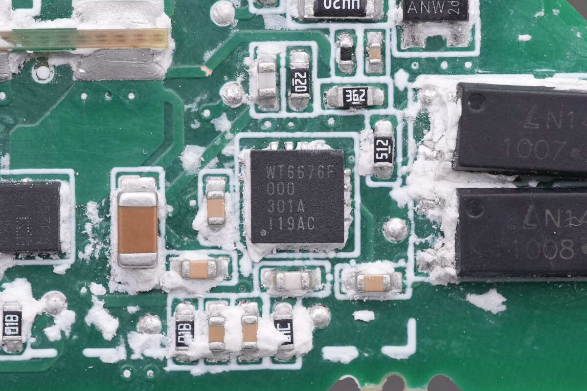
The USB PD protocol chip is from Weiquan, model WT6676F. It is a protocol chip that supports USB PD3.1 . It supports 36V output voltage, supports programmable constant voltage and constant current control, and integrates a low-side current sampling amplifier internally to support line loss compensation. . WT6676F supports programmable protection functions and supports overvoltage, undervoltage, overcurrent and overheating protection.
The chip has a built-in 10-bit ADC for voltage and current detection, a built-in NMOS load switch driver, a built-in output discharge tube, a built-in power supply voltage regulator, supports PFC control, supports energy-saving mode, the input voltage can reach 45V, and is packaged in QFN-16. Weld a thermistor on the right side of the chip to detect the internal temperature of the charger and provide overheating protection.
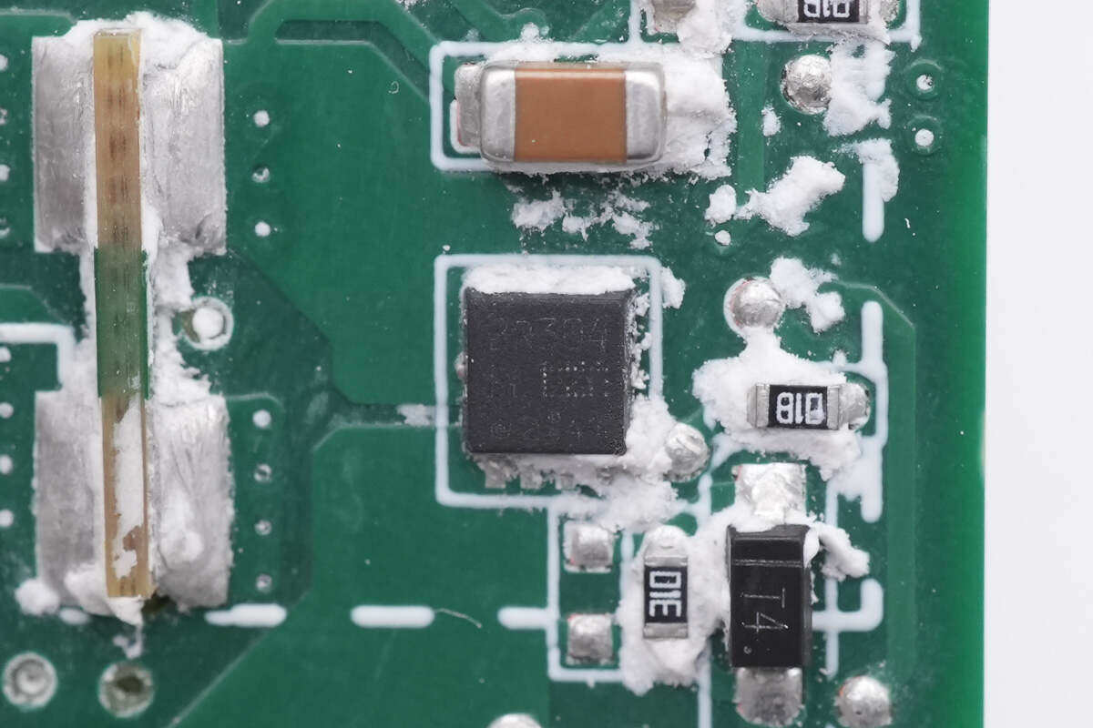
The output VBUS switch tube is from Toshiba, model TPN2R304PL. It is a 40V NMOS with a resistance of 1.8mΩ and is packaged in TSON Advance.
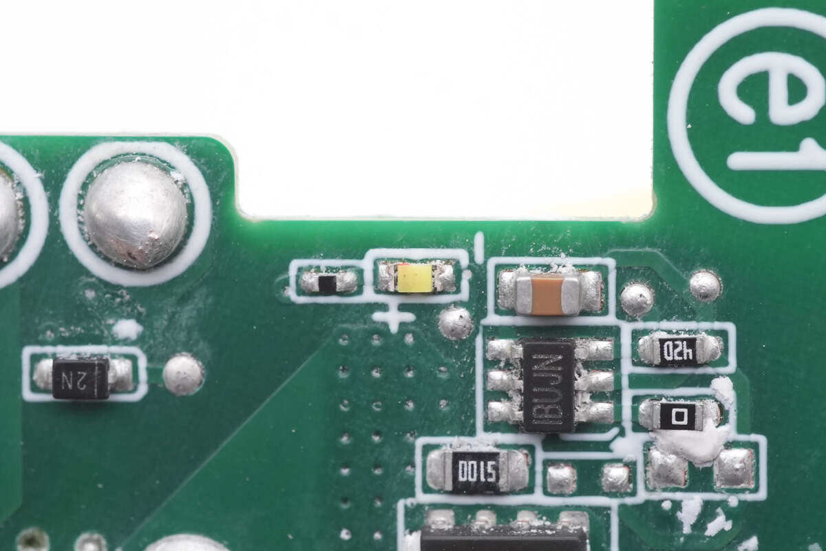
SMD LED lights are used for power indication.
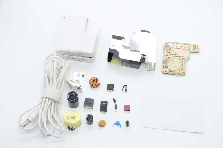
Take a look at all the disassembly and take a family photo.
Summary of disassembly of charging head network
Dell’s notebook power adapter is designed with its own output line. It comes with a 1.8-meter long USB-C output line. It supports Dell’s 28V 5.85A 165W , 20V 6.5A 130W private protocols, and supports 140W PD3.1 specifications. It can not only meet the power supply needs of Dell graphics workstations, but also meet the power supply needs of other notebooks. The adapter uses a Torx interface for power supply and is equipped with a power indicator light.
Charging Head Network learned through disassembly that Dell’s notebook power adapter uses active rectification and uses NXP TEA2206T controller with Fuding advanced MOS. The adapter uses PFC+HFB topology, the PFC controller uses TEA19162, and uses Infineon IGLD60R070D1 gallium nitride switch tube, and uses Yangjie ultra-fast recovery diode rectification.
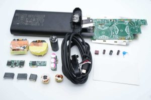
The HFB controller is from Infineon and is a customized model. The synchronous rectification controller uses MPS MP6951, and the protocol chip uses Weltrend WT6676F. The internal capacitors of the adapter are from Wanyu and Jinshan brands. The PCBA module is integrally filled with glue. The PCBA module is wrapped with aluminum heat sinks to increase the heat dissipation area. The internal heat dissipation performance of the adapter is optimized for long-term high-power output scenarios such as laptop charging to reduce the temperature rise of long-term output.

