Teardown report: CISCO Cisco 18W RJ45 to USB-C power adapter AN18A-59CB
Preface
Charging Head Network has obtained a USB-C power adapter launched by Cisco . This adapter has a USB-C interface and an RJ45 network interface. When in use, connect the network cable to the adapter, and then connect it to the conference phone through the USB-C cable to provide power to the Cisco 8832 conference phone and the wired network at the same time.
This adapter uses fixed US pins and supports global wide voltage input. It also has 18W PD fast charging output, supporting 5V3A, 9V2A and 12V1.5A output power. Let’s take a look at the disassembly of this USB-C interface power adapter and take a look at the internal design and materials used.
Cisco RJ45 to USB-C power adapter appearance
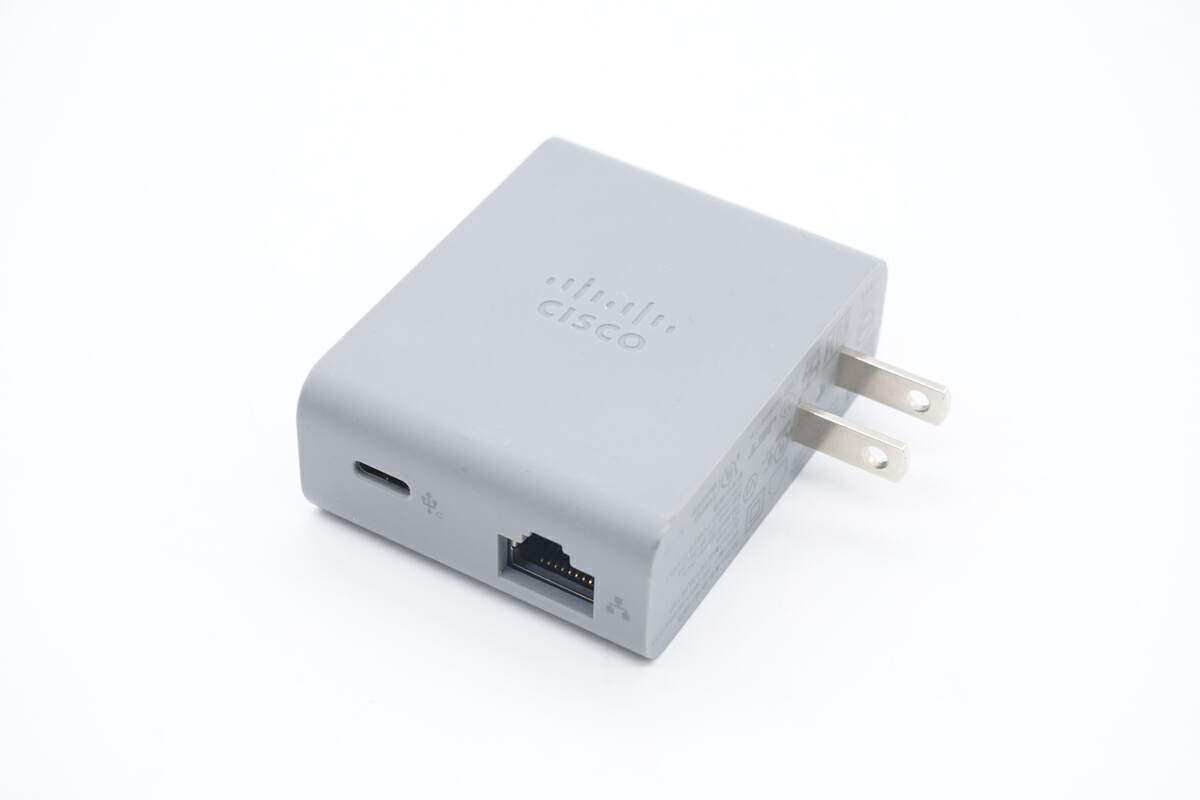
This power adapter from Cisco adopts a gray tone shell, and the surface of the body is frosted to effectively resist fingerprints. The bottom pins are perpendicular to the length of the fuselage. This design may cause the adapter to take up more space when plugged into the socket, squeezing out the space for other holes.
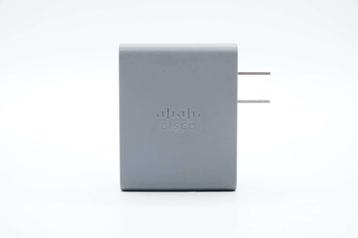
The CISCO brand logo is designed in the center of the front of the fuselage.
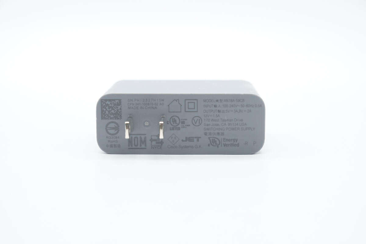
The bottom shell has detailed specifications of the power adapter printed on it.
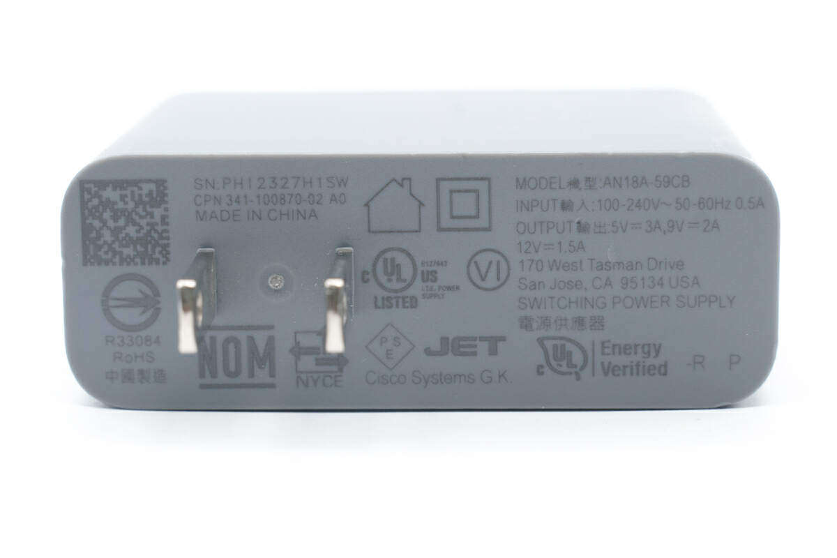
Close-up of power adapter parameters
Model: AN18A-59CB
Input: 100-240V~50/60Hz 0.5A
Output: 5V3A, 9V2A, 12V1.5A
This adapter has passed UL, PSE, NOM, NYCE certification, and Level VI energy efficiency certification.
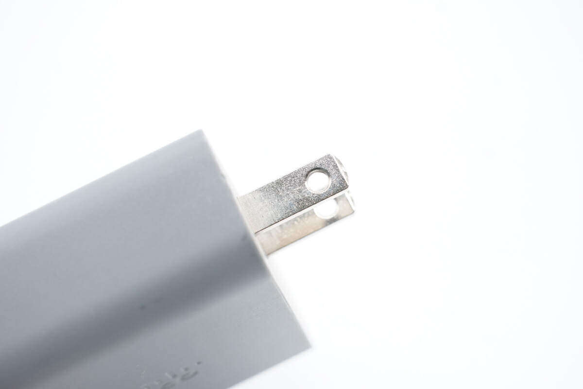
The adapter is equipped with fixed US pins.
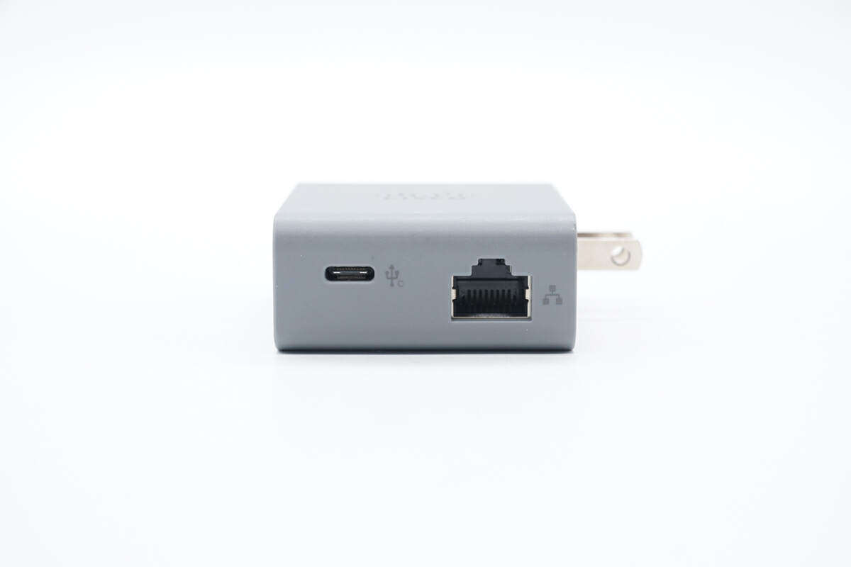
One end of the fuselage is equipped with USB-C and RJ45 sockets.
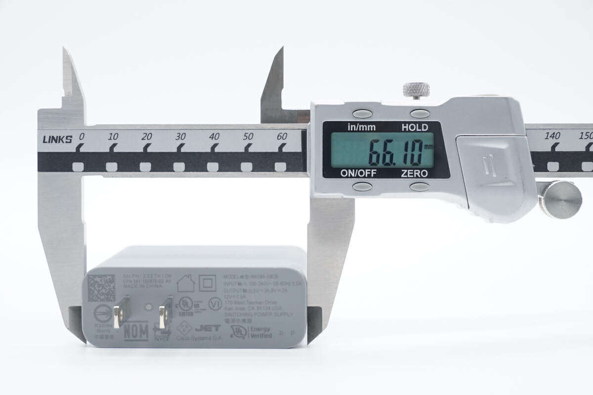
The measured length of this power adapter is 66.1mm.
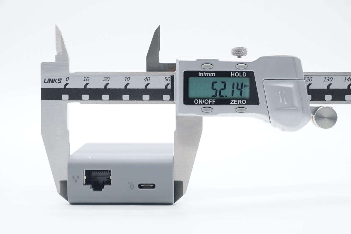
The height is 52.14mm.

Thickness is 24.22mm.
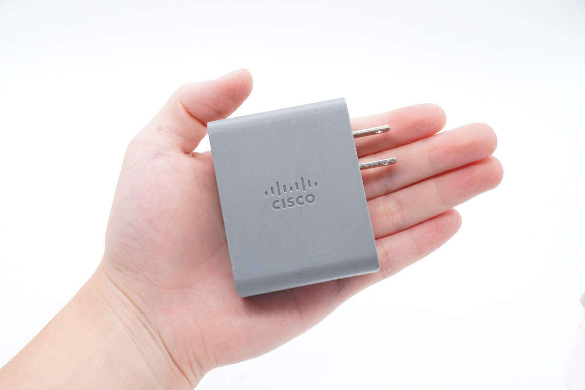
You can intuitively feel the size of the product in your hand.
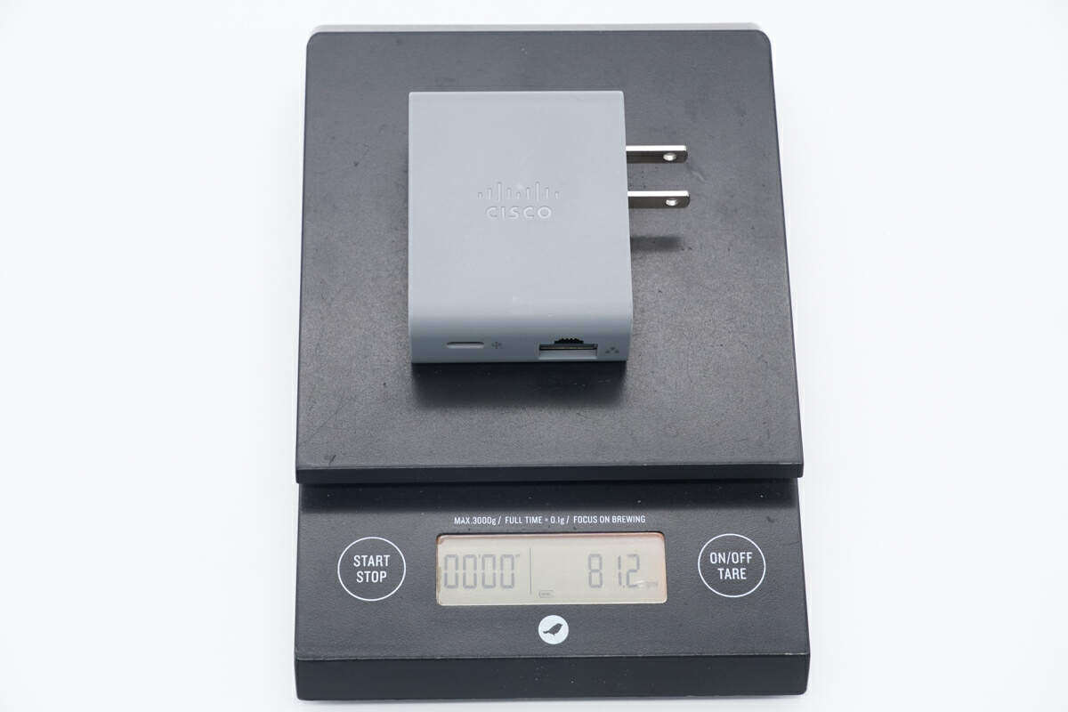
In addition, the measured weight of the power adapter is about 81g.
Cisco RJ45 to USB-C power adapter appearance
After looking at the appearance of this power adapter, let’s start to disassemble it and take a look at the internal materials and design.
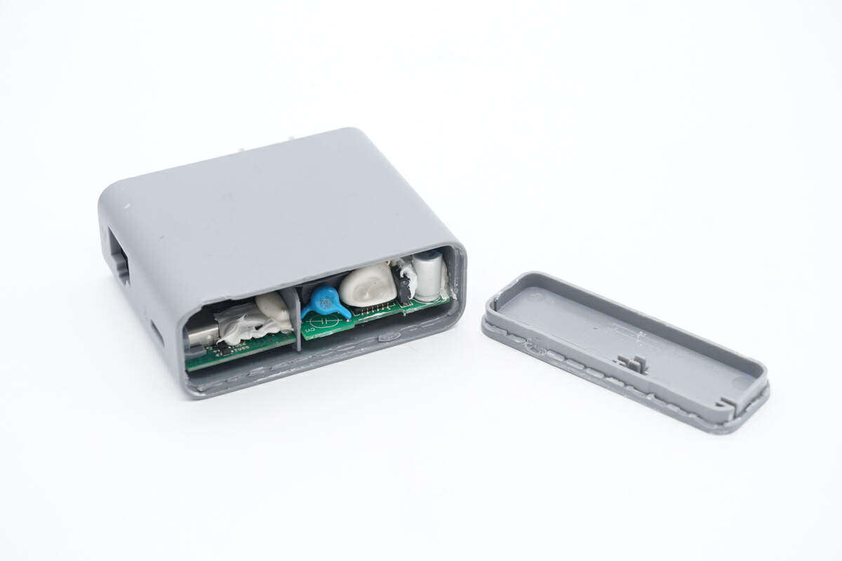
First pry open the cover on the top of the adapter to see the PCBA module inside.
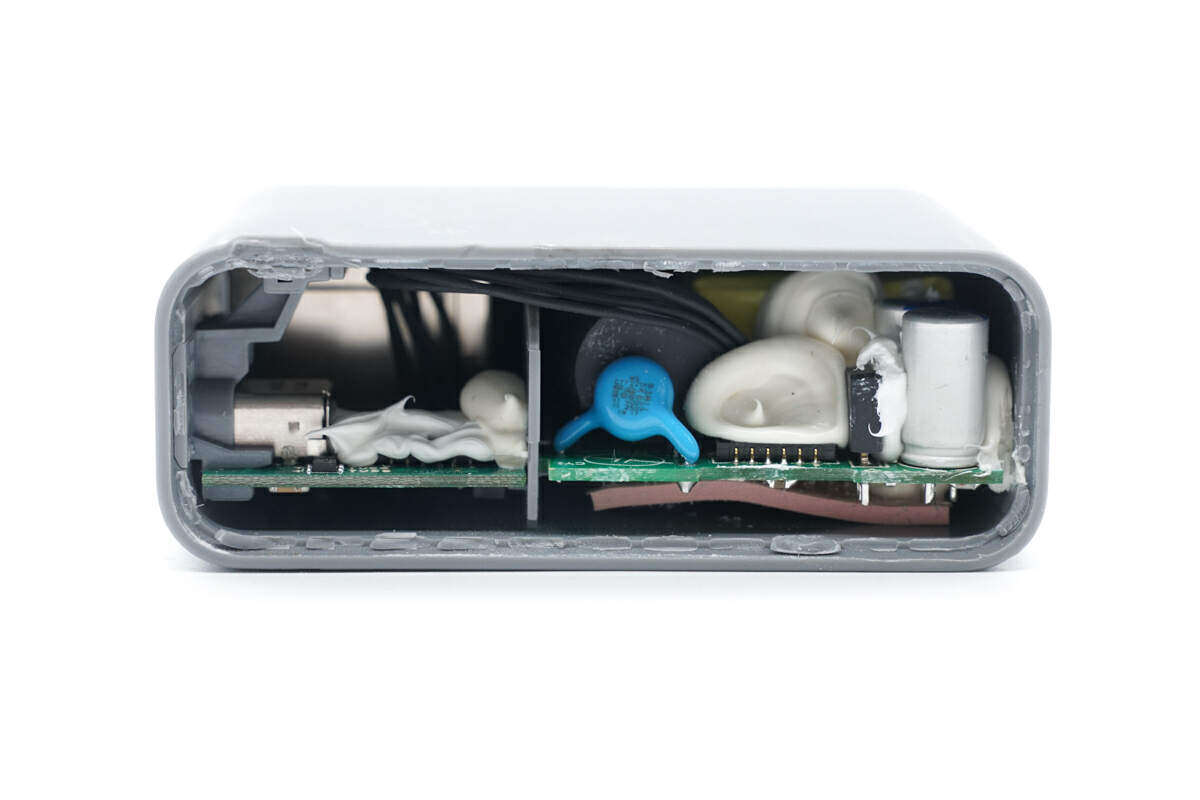
There is an isolation cabin inside the casing, which is divided into two parts to place the PCBA module.
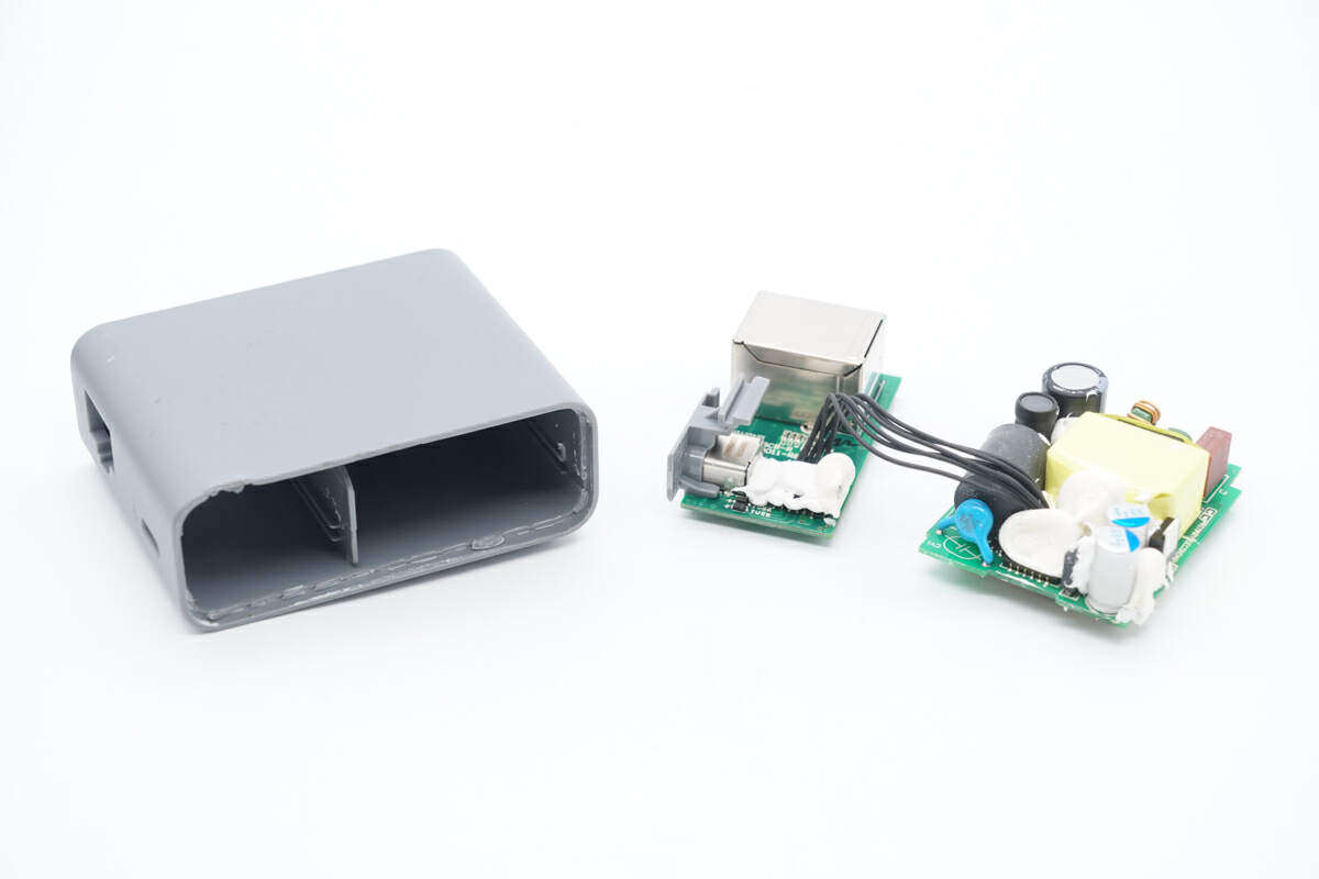
Pull out the internal PCBA module and connect the two internal PCBs through wires.
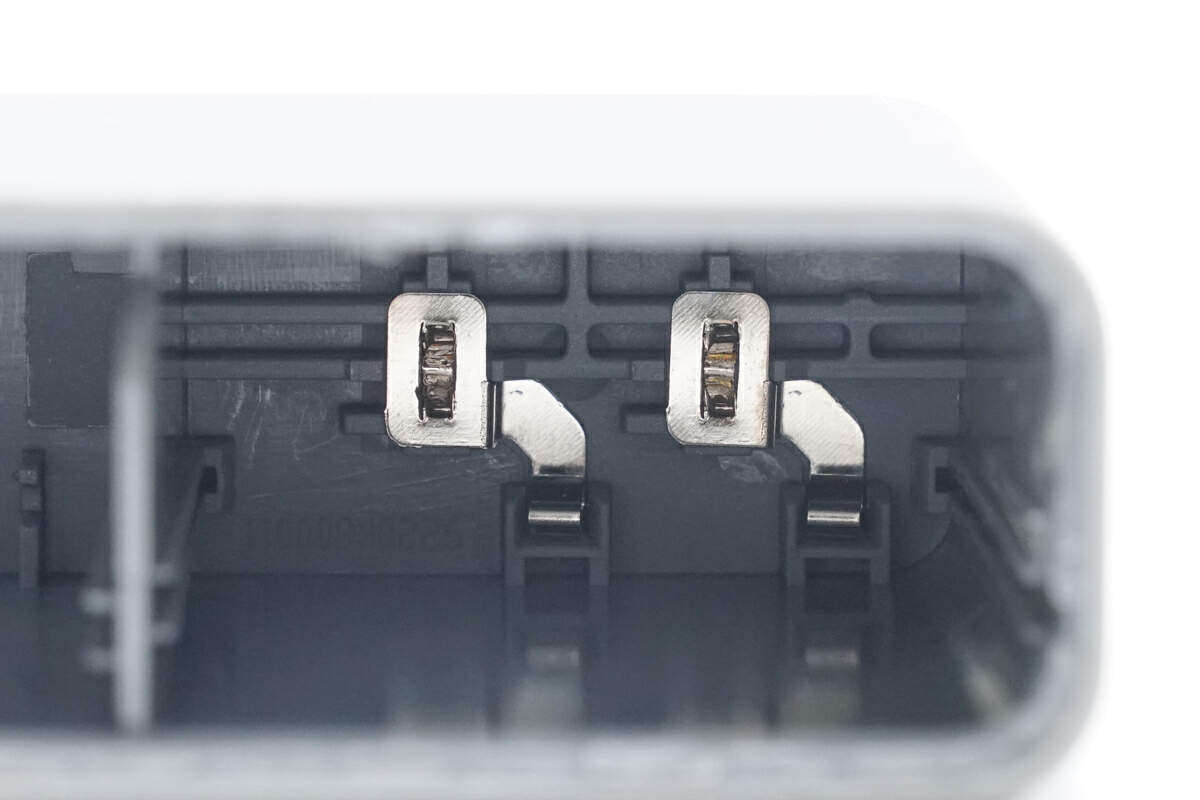
The AC input pin is pressed against a spring to power the PCBA module, and a card slot is provided inside the housing to fix the PCB.
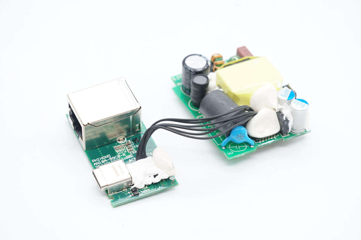
The two PCBs are connected via wires for power supply.
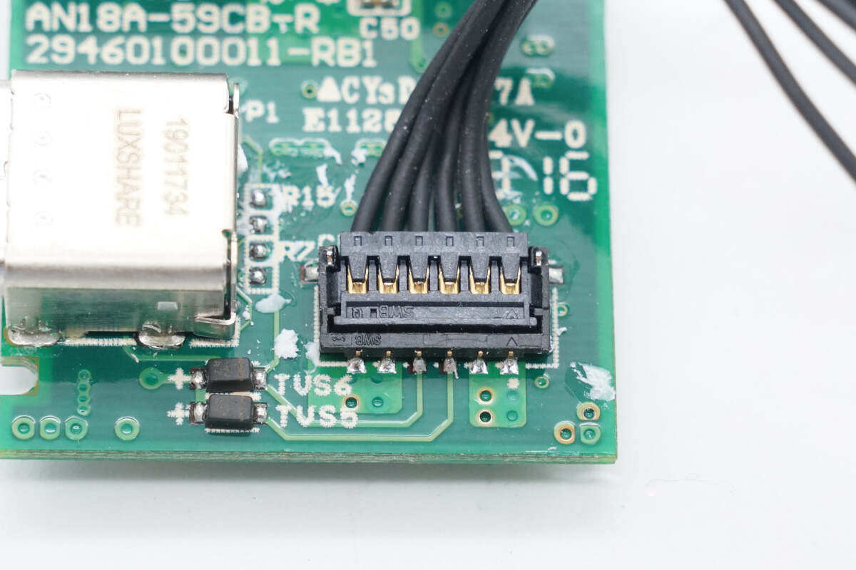
Close-up of the socket connected to the small board. The six wires are the positive, negative and CC wires.
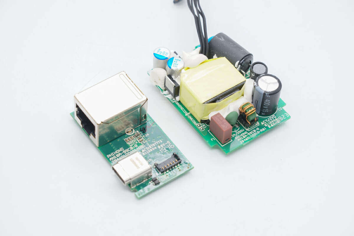
Disconnect the connecting wires and separate the connections between the two PCBs.
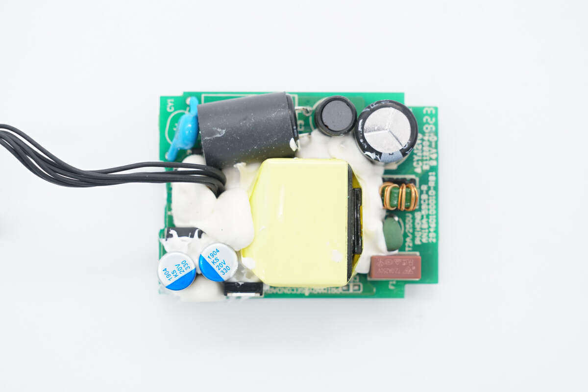
Let’s look at the power adapter part first.

The other end of the connecting wire is filled with glue and fixed.
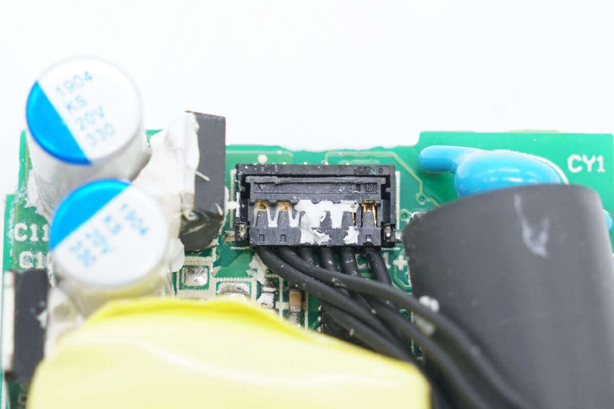
The same socket structure is also used on the adapter end.
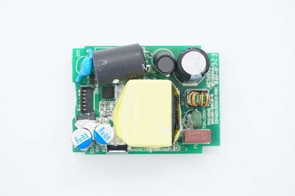
An overview of the power adapter PCBA module. On the right side are the AC input terminals, welding fuses, NTC thermistors, common mode inductors, and high-voltage filter capacitors. Solder the transformer to the left. Above the transformer are the high-voltage filter capacitors and differential mode inductors. On the upper left side are the blue Y capacitors and output sockets. In the lower left corner are the output filter capacitors and synchronous rectifier tubes.
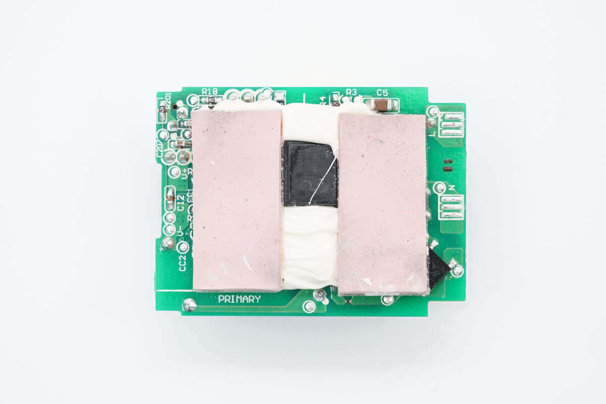
The back of the PCBA module is coated with thermal conductive glue and two thermal pads are attached.
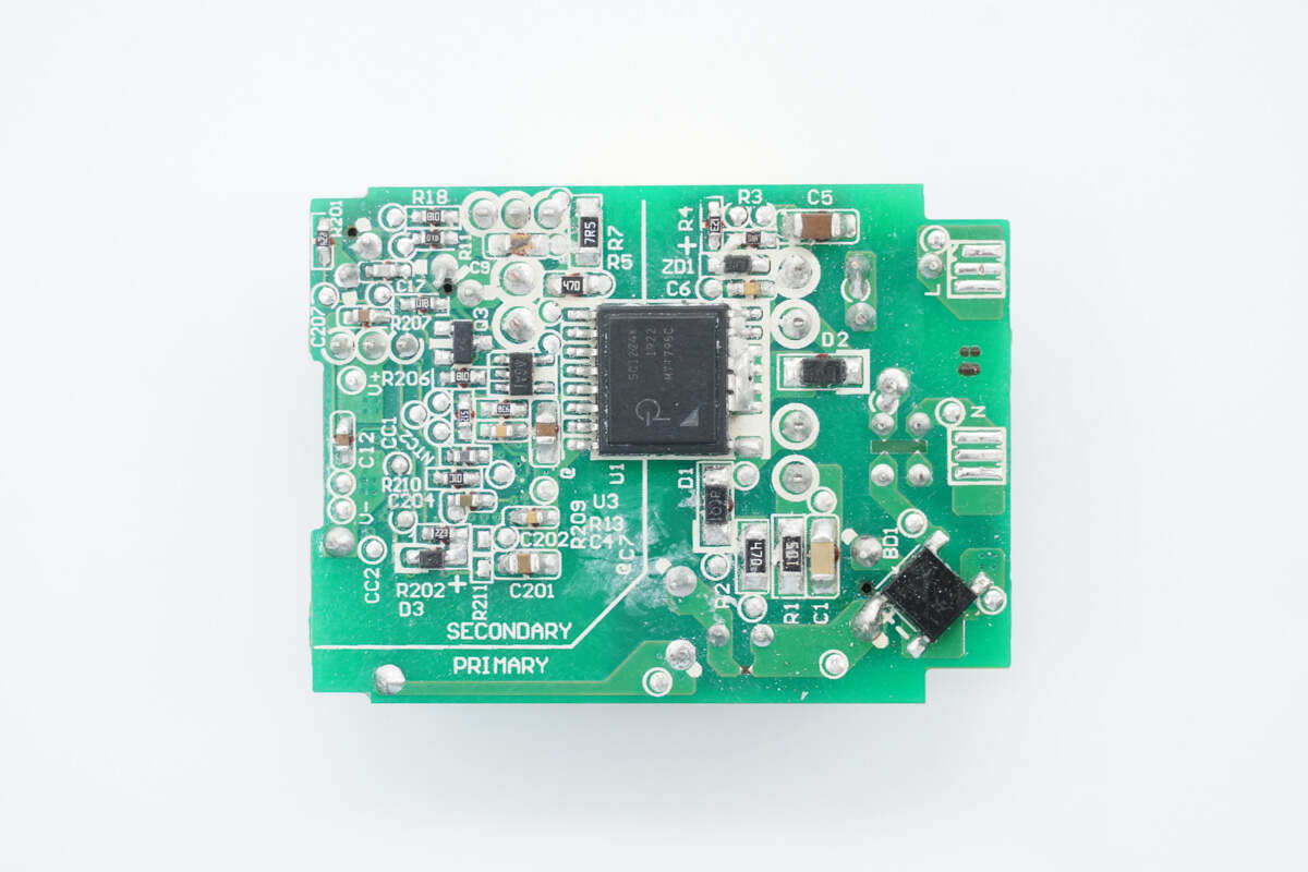
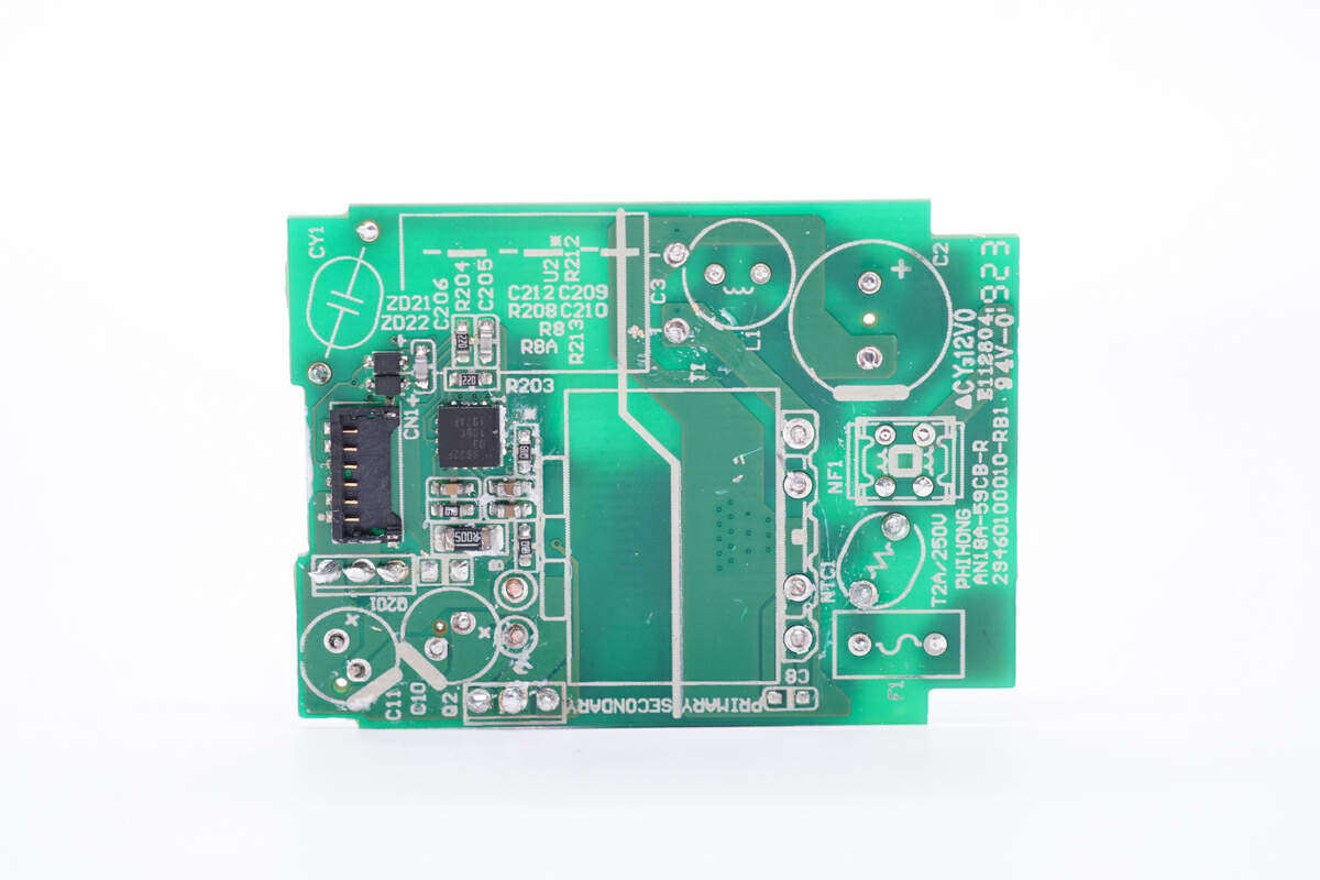
Clean off the filled glue and solder a power chip and rectifier bridge on the back.
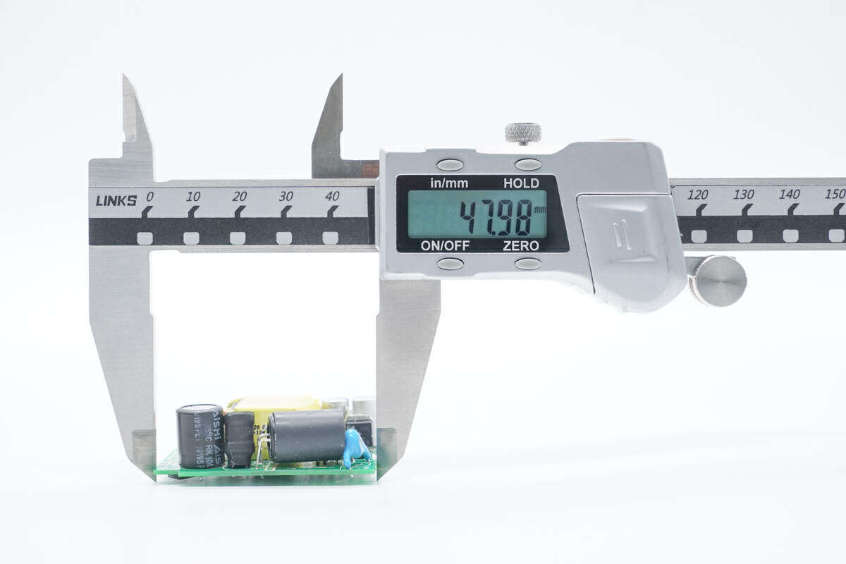
The length of the PCBA module measured using a vernier caliper is approximately 47.98mm.
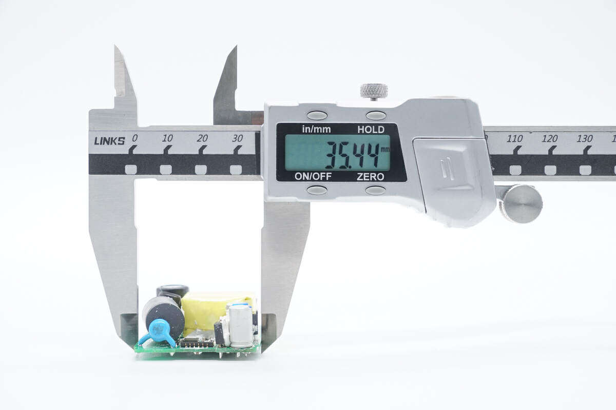
PCBA module width is approximately 35.44mm.
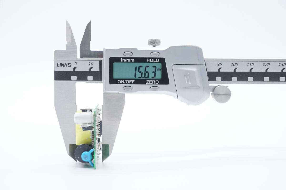
The PCBA module thickness is approximately 15.6mm.
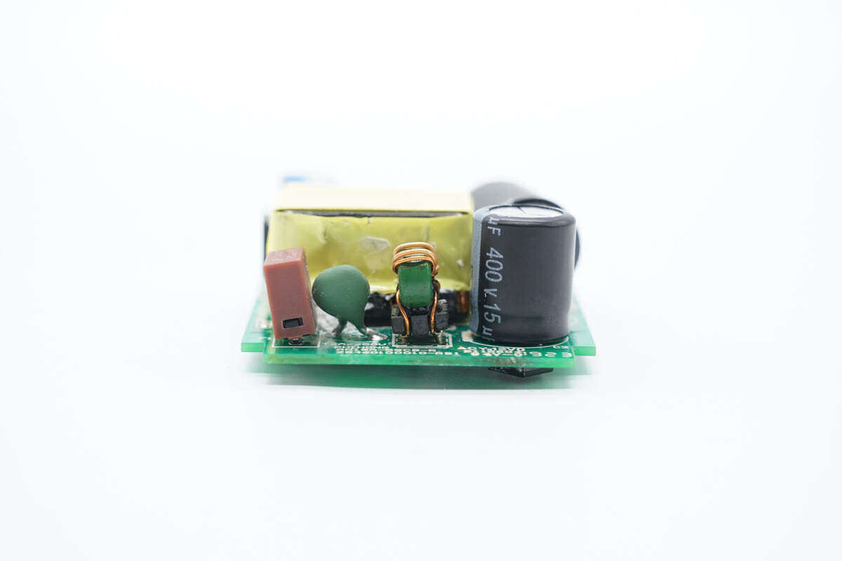
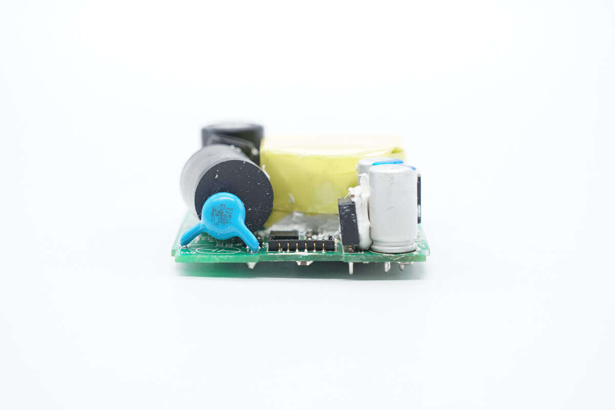
At a glance from the side of the PCBA module, welding fuses, NTC thermistors, common mode inductors and high voltage filter capacitors.
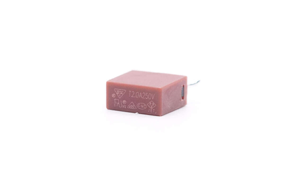
The input fuse specification is 2A 250V.
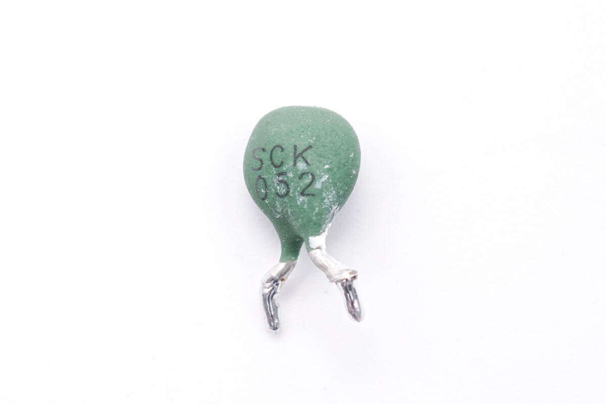
The SCK052 NTC thermistor is used to suppress power-on surge current.

The common mode inductor is wound with enameled wire and insulated wire, with an insulating bracket welded to the bottom.
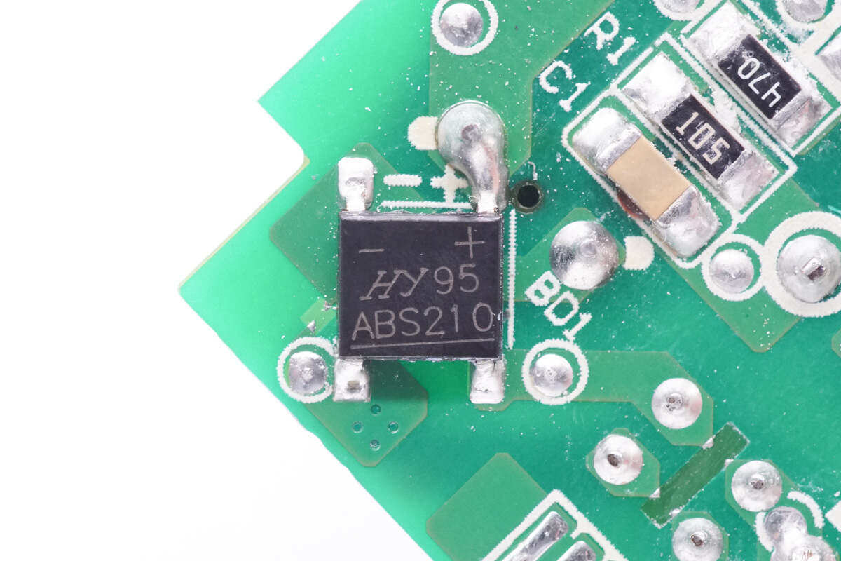
Rectifier bridge model ABS210, specification is 2A 1000V.
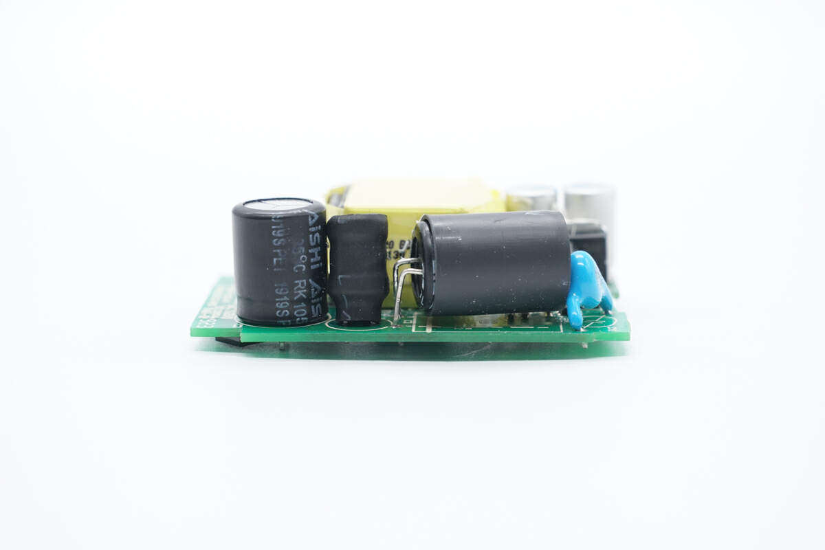
The high-voltage filter capacitor and differential mode inductor are welded on the side of the PCBA module, another high-voltage filter capacitor is covered with an insulating sleeve, and the Y capacitor is welded on the right side.
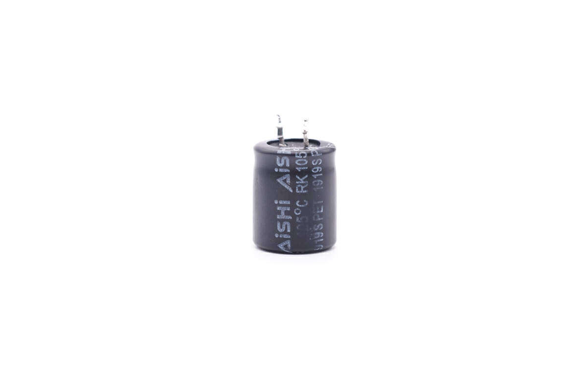
The high voltage filter capacitors are from Aihua.
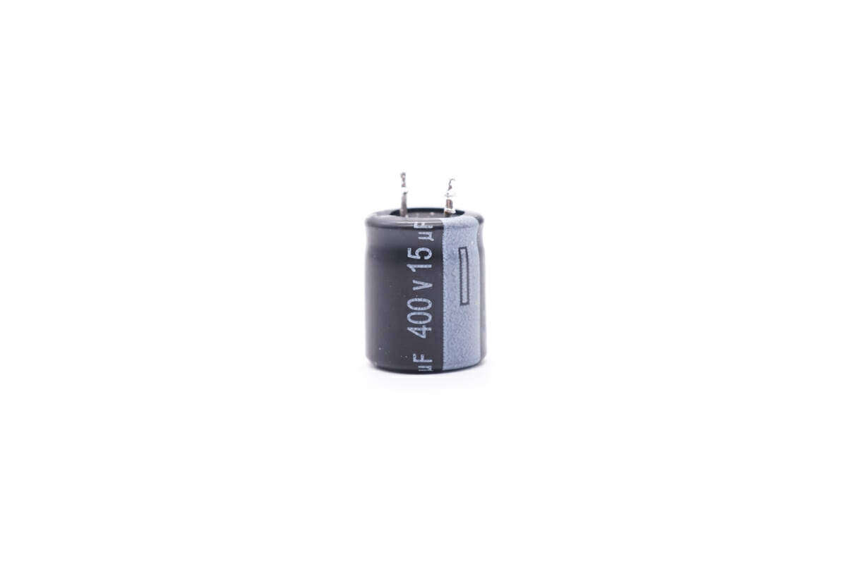
Specification is 400V15μF.
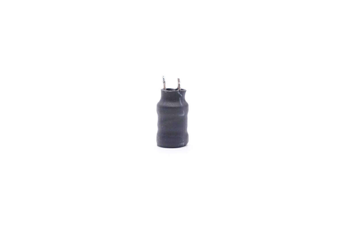
Differential mode inductors are wrapped with heat shrink tubing for insulation.
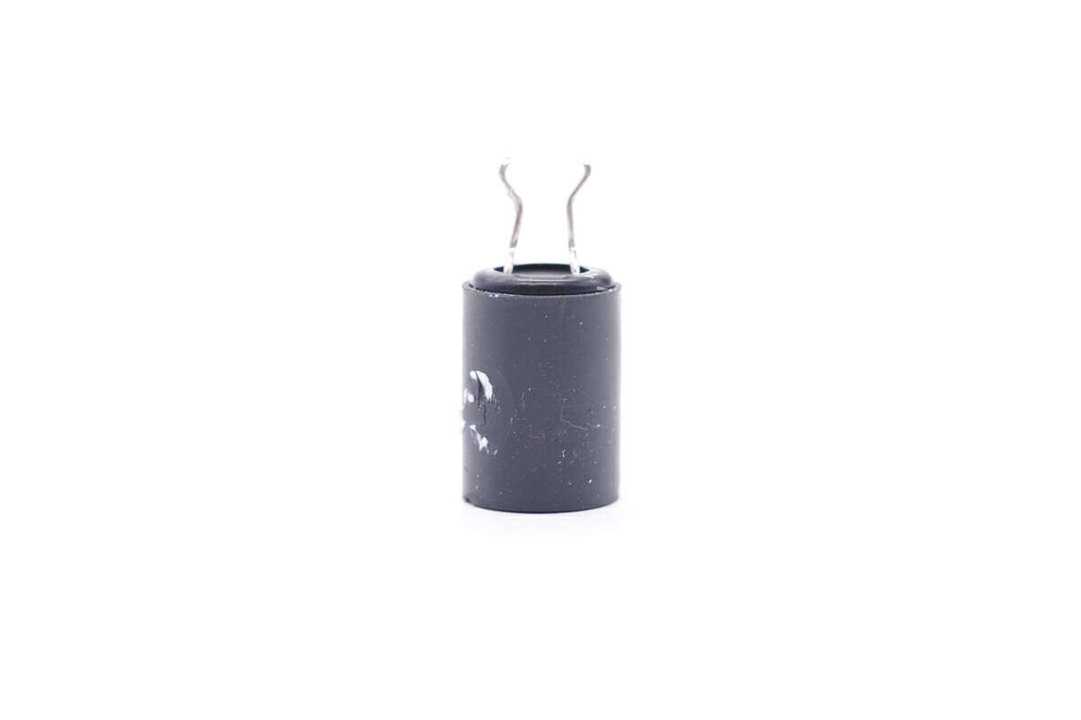
Another electrolytic capacitor is coated with an insulating sleeve.
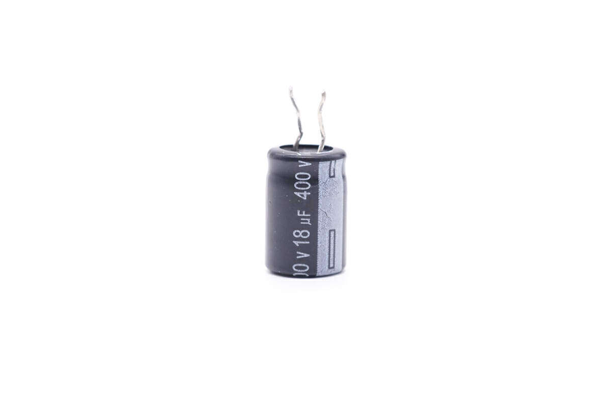
The capacitor specification is 400V18μF.
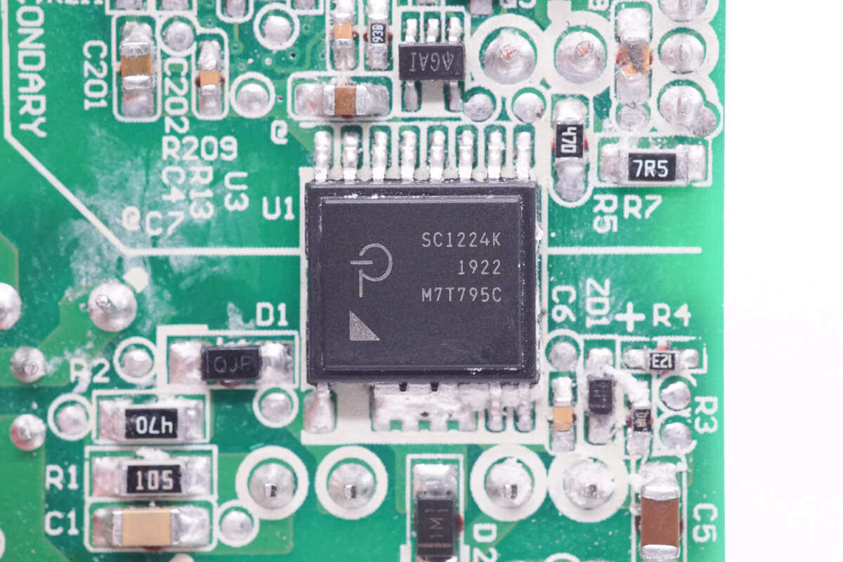
The power main control chip is from PI, model SC1224K. The chip integrates the primary controller, primary switch tube, feedback and synchronous rectification controller.
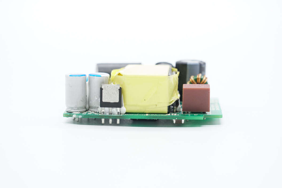
Weld the output filter capacitor, synchronous rectifier and transformer on the side.
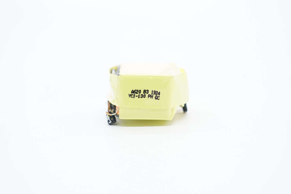
The transformer core is tightly wrapped with tape insulation.
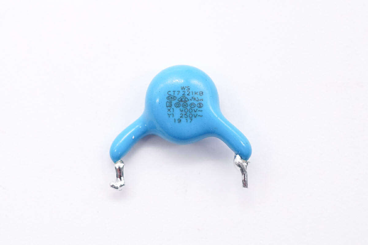
Close-up of blue plug-in Y capacitor.
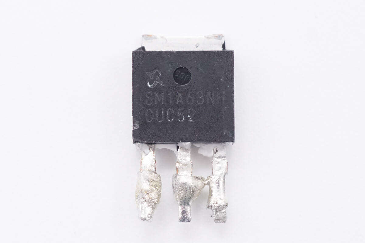
The synchronous rectifier is from Dazhong, model SM1A63NH, NMOS, withstand voltage 100V, conduction resistance 9.6mΩ, and adopts TO251S package.
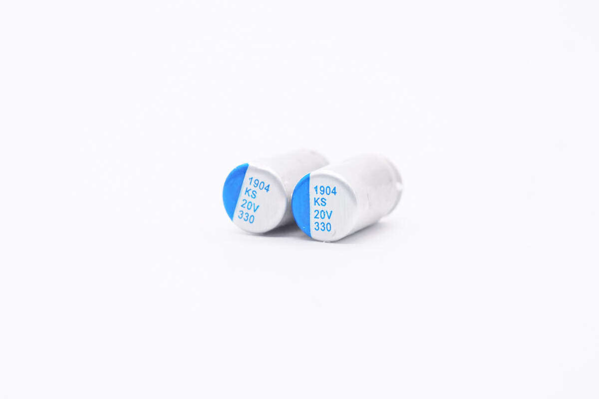
The output filter capacitor is from Dongjia and is a KS series solid capacitor with a specification of 20V 330μF.
Weld the output socket and VBUS switch tube at the output end.
Remove all the direct plug-in components on the front of the PCBA module and solder a protocol chip.
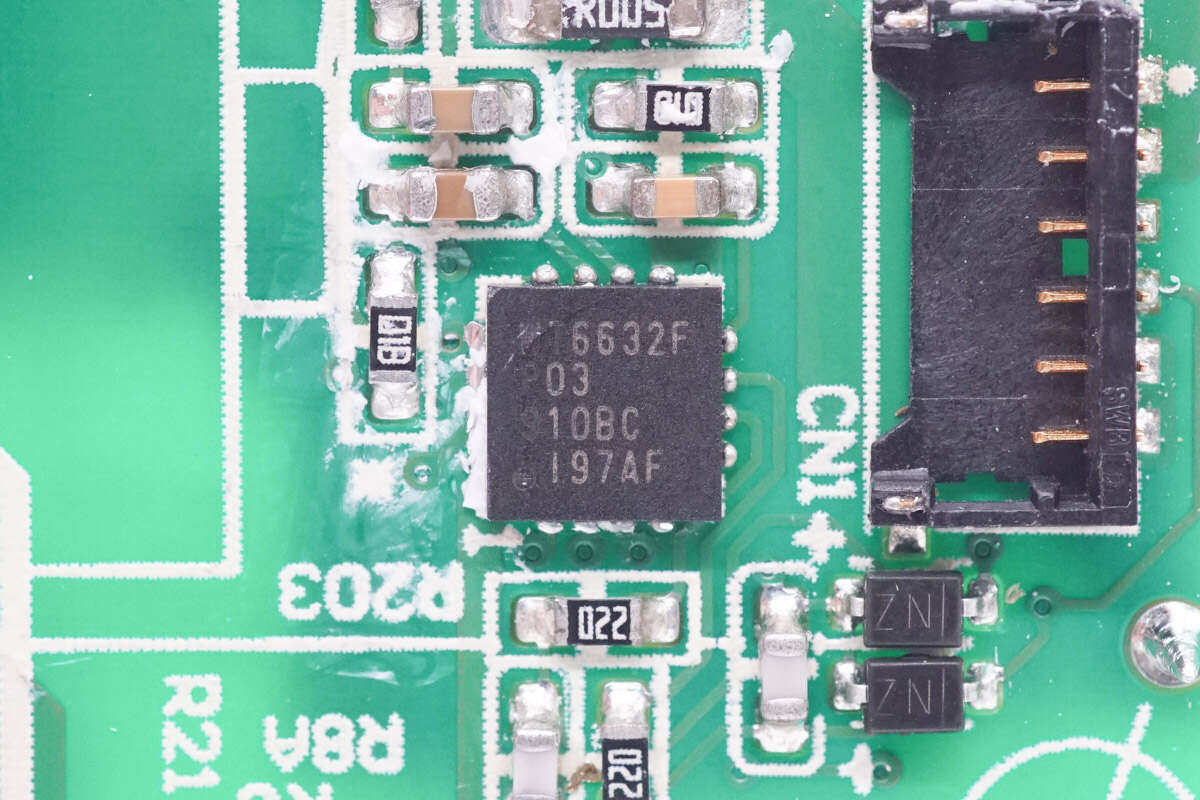
The output protocol chip is from Weltrend, model WT6632F. This chip has passed USB PD3.0 certification. As a highly integrated USB PD controller, it supports the USB PD3.0 specification, supports a wide operating voltage range from 3V to 30V, and is designed for chargers, mobile power supplies and other output devices.
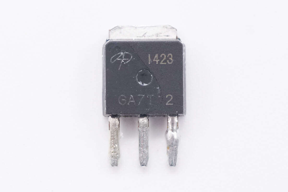
The output VBUS switch is from AOS, model AOI423. It is a PMOS with a voltage resistance of 30V, a conduction resistance of 6.2mΩ, and a TO251A package.
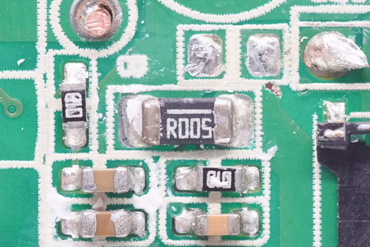
The 5mΩ sampling resistor is used to detect the output current.
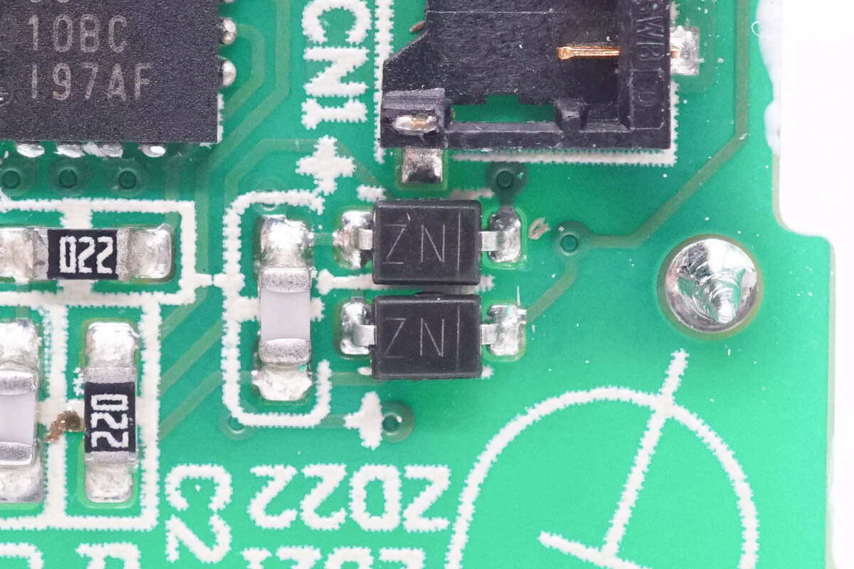
Two ESD diodes are used for static electricity protection of CC pin.
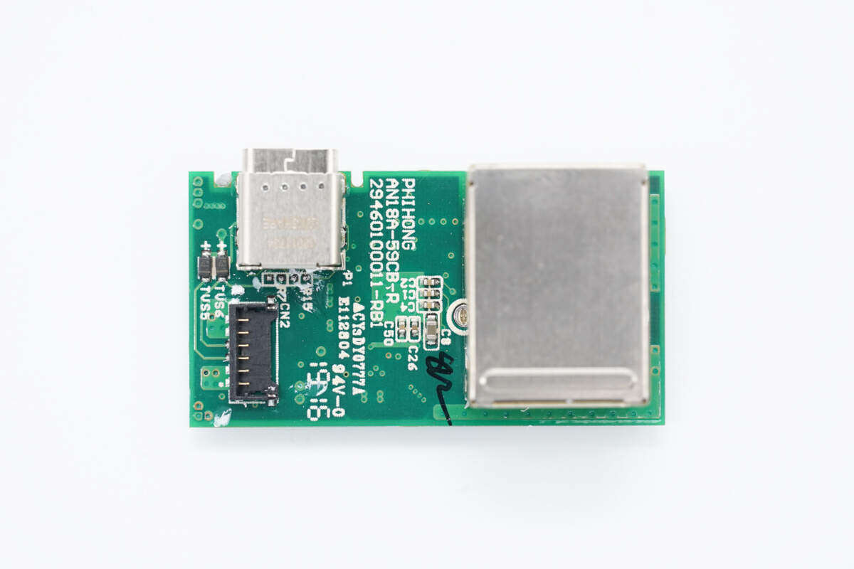
The USB-C female socket, power connection socket and RJ45 network interface are soldered on the front of the interface board.
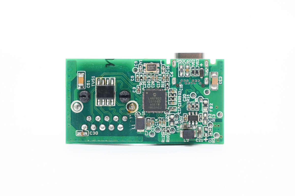
The network conversion chip and memory are soldered on the back of the small board.
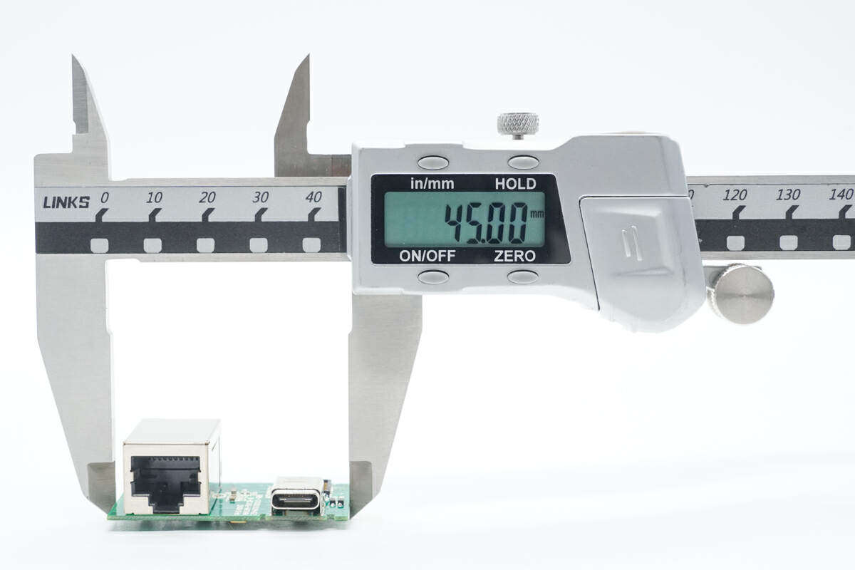
The length of the PCBA module measured using a vernier caliper is approximately 45mm.
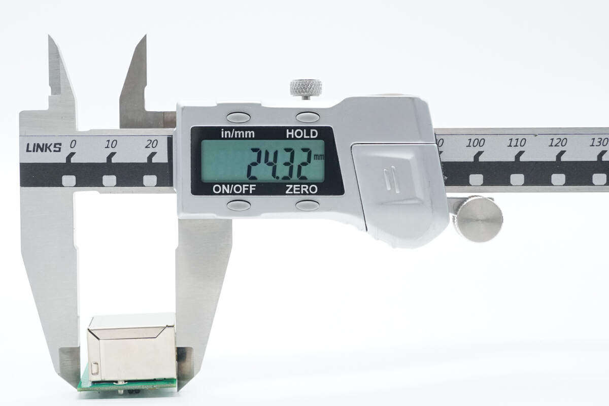
The width is approximately 24.32mm.
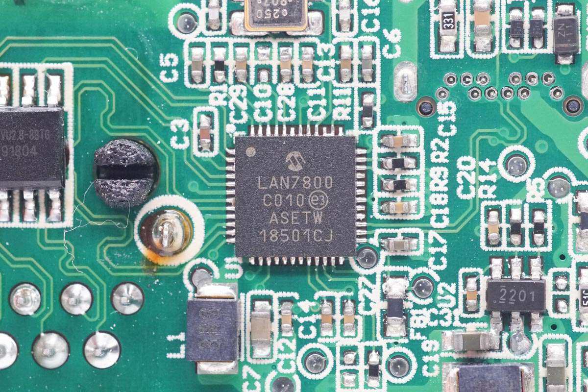
The network conversion chip is from Microchip Technology, model LAN7800. It is a USB3.1 to Gigabit Ethernet controller. It is a single-chip design, backward compatible with 5Gbps, 480Mbps and 12Mbps modes, and supports a variety of advanced functions, suitable for USB to Ethernet adapter and other applications.
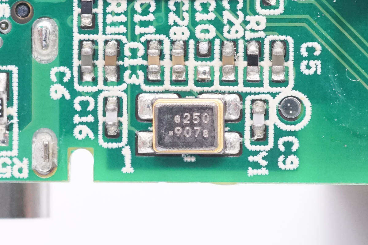
Close-up of the external 25.000MHz clock crystal oscillator of the network conversion chip.
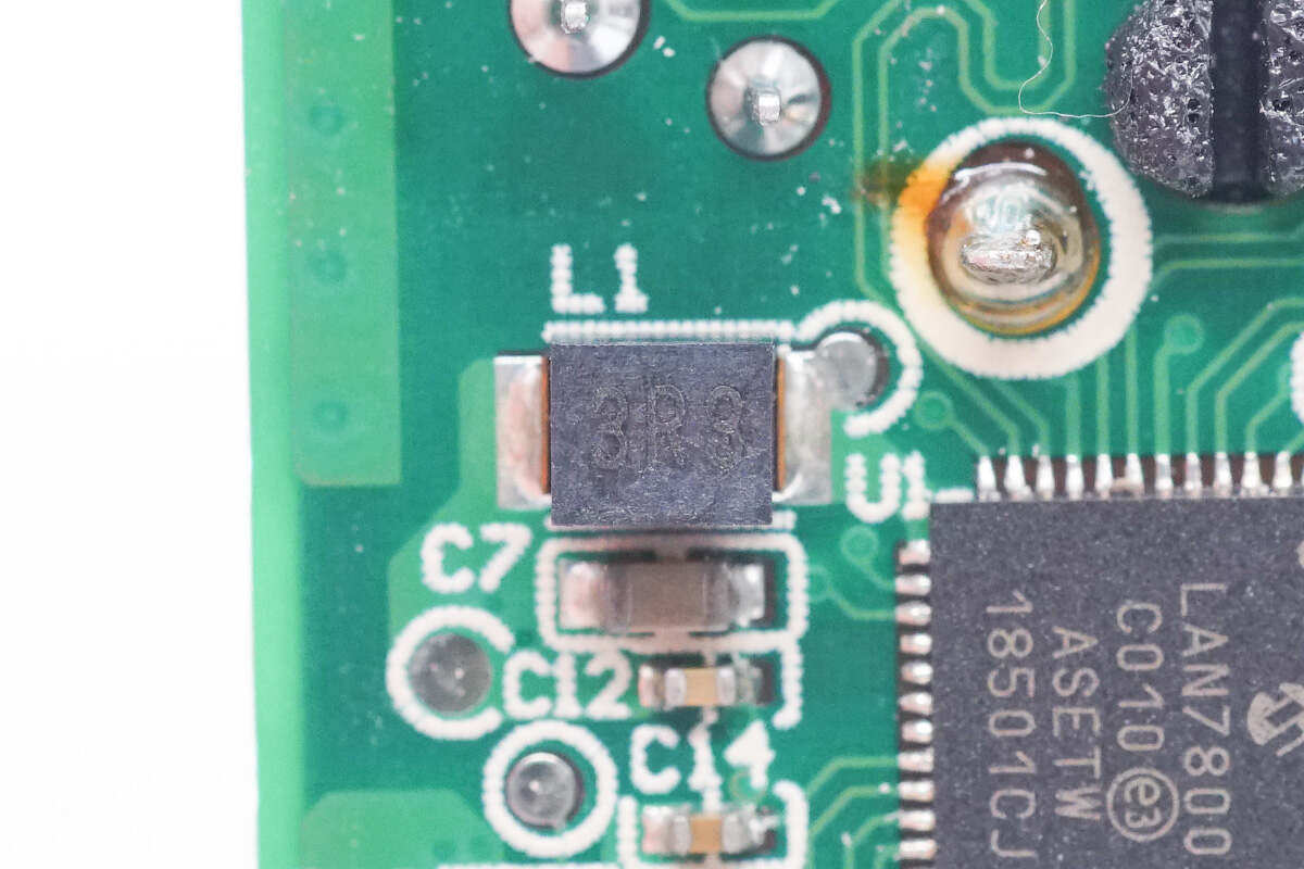
Close-up of the external buck inductor of the network conversion chip.
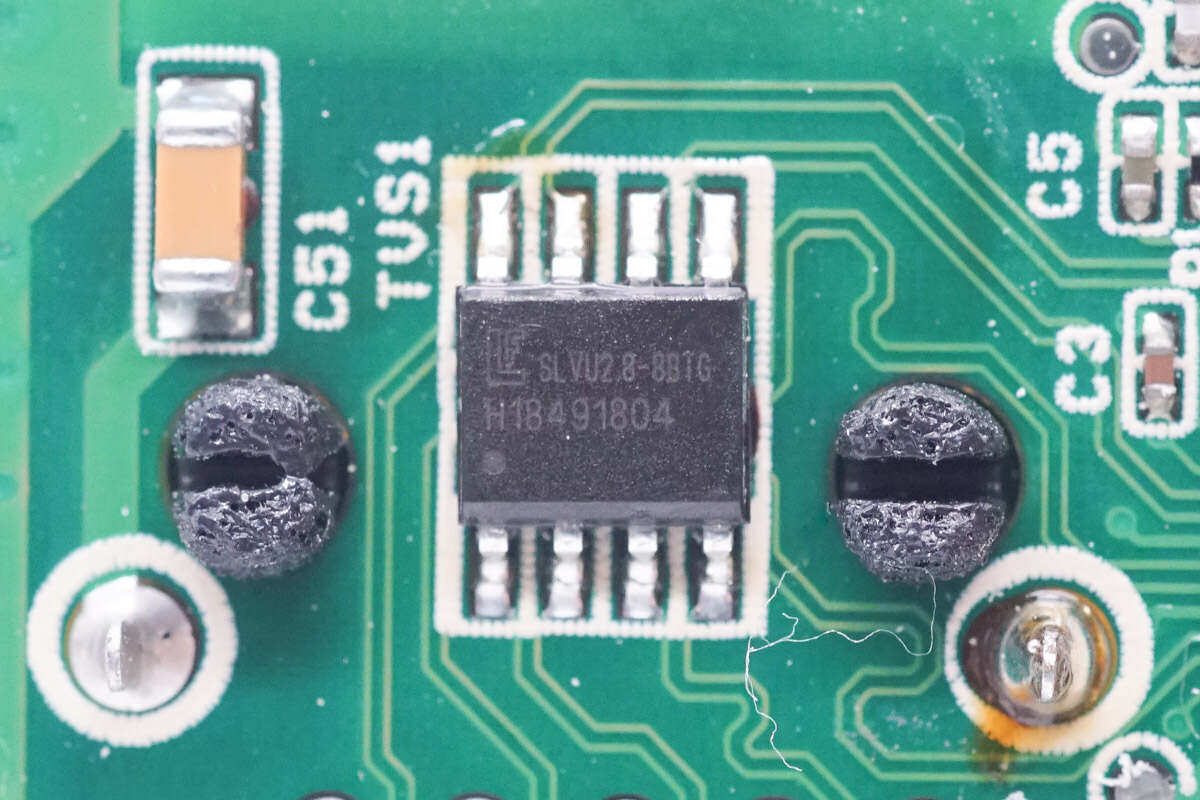
The ESD protection chip is from Littel, model SLVU2.8-8BTG, used for electrostatic surge protection of Gigabit Ethernet interfaces.
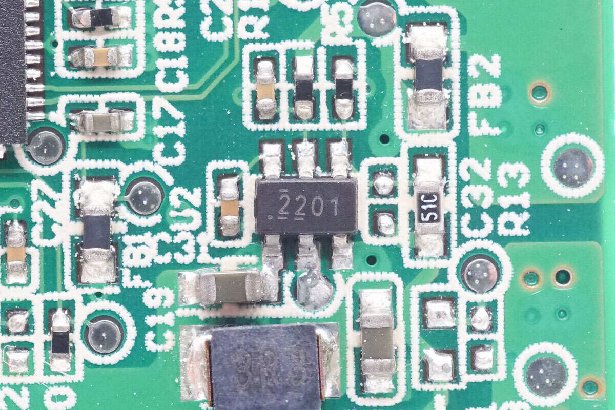
The buck chip that powers the network conversion chip comes from TI Texas Instruments, model TPS562201. It is a 17V input synchronous buck converter with an output current of 2A and an internal integrated switch tube.
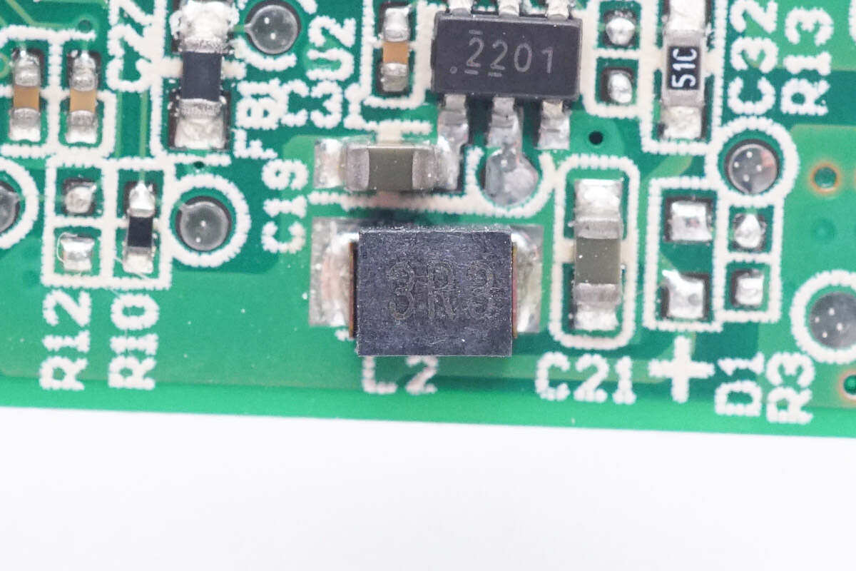
Close-up of the buck inductor.
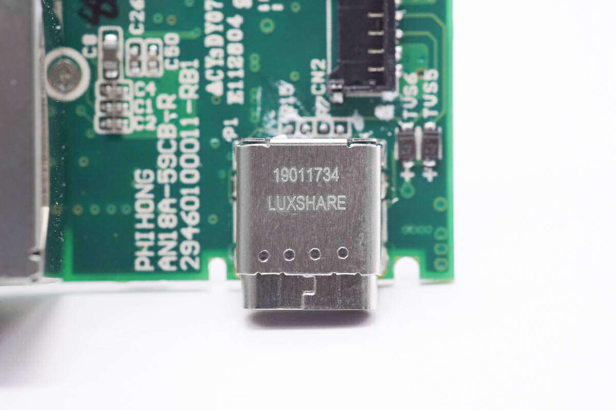
The USB-C female socket comes from Luxshare Precision.
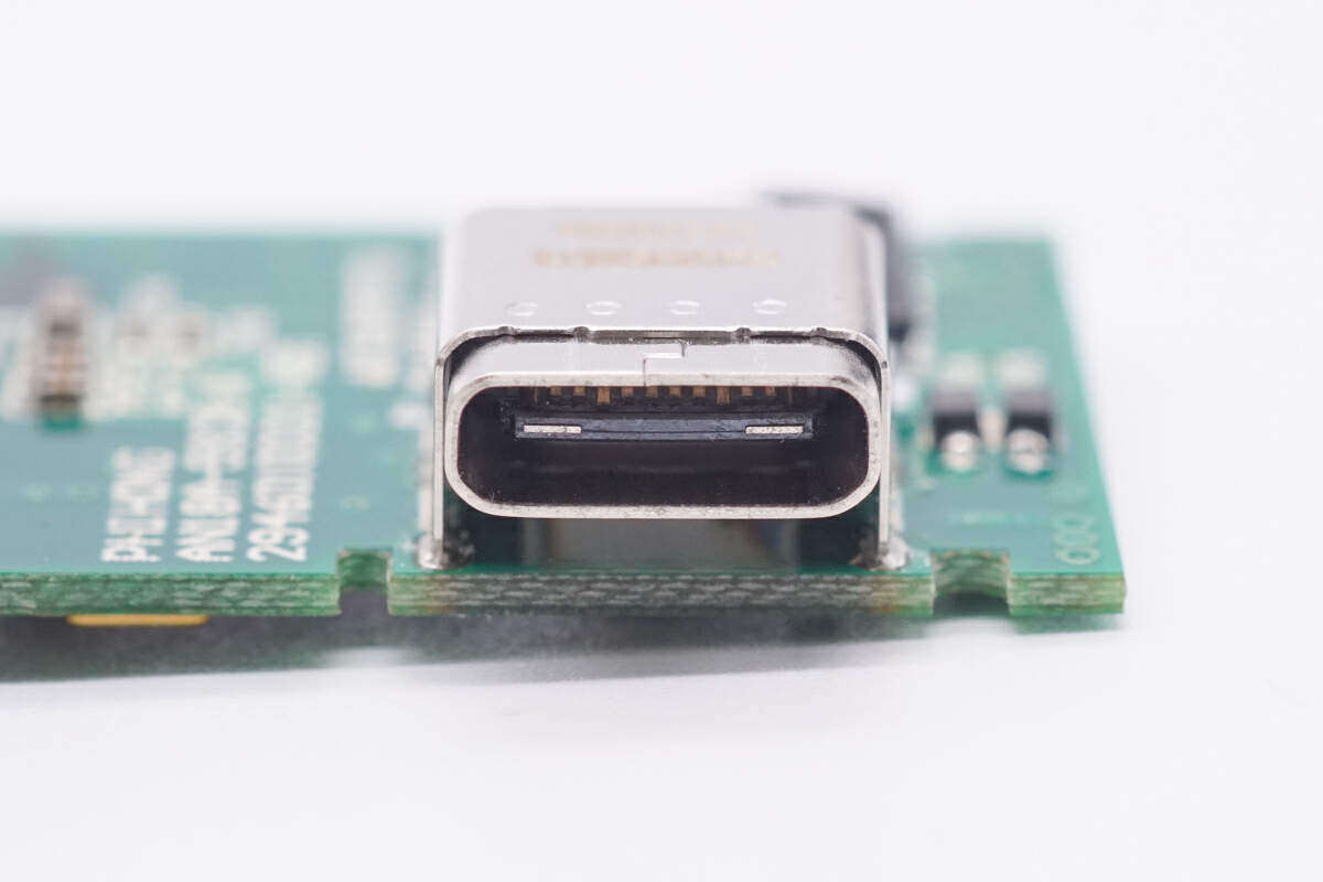
The female base is reinforced with a metal shell.
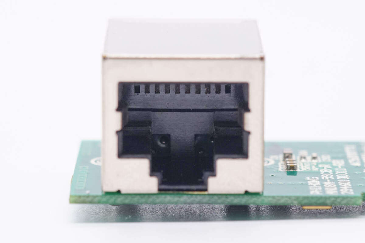
The RJ45 network interface is shielded by a metal shell.

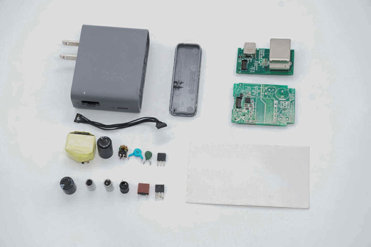
Take a look at all the disassembly and take a family photo.
Summary of disassembly of charging head network
Cisco’s USB-C power adapter has a USB-C interface and an RJ45 network interface, and has fixed US pins. The power adapter supports global wide voltage input, and the USB-C interface supports 5V3A, 9V2A and 12V1.5A output. The adapter connects to the network through a network cable, and provides both power and network connectivity to the conference phone by connecting the USB-C cable to the Cisco 8832 conference phone.
Charging Head Network learned through disassembly that Cisco’s USB-C power adapter consists of two PCBs, divided into a power adapter module and a network connection module, connected by wires in the middle. The power adapter module uses PI SC1224K main control chip, paired with Weltrend WT6632 protocol chip, and the network conversion chip uses Microchip Technology LAN7800. The power adapter module is attached with a thermal pad to enhance heat dissipation, and the internal workmanship is made of reliable materials.

